9
\$\begingroup\$

For a hobby project of mine, I'm thinking about connecting some old 5V SRAM chips like this one to a 3.3V - capable FPGA. The target frequency is 50MHz. After some simulator experiments I found out that a simple voltage divider could work:
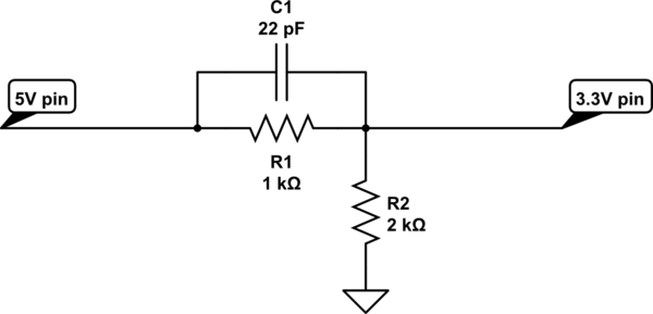
schematic

simulate this circuit – Schematic created using CircuitLab

This gives a nice 0.2..3.0V peak to peak signal on the 3.3V side when driven by 5V side. In the opposite direction however, the output signal is only 0.4..2.6V peak to peak, which is kind of within the spec for a W24512AK (\$V_{0H}=0.8V\$ and \$V_{1L}=2.2V\$) but the margin isn't great. I wonder if this will work at all in practice.

So I'd like to improve the margin by using an active level converter, but as far as I can see, all simple schematics (e.g. the ones listed here) have a terrible frequency response. The only viable solution I see is to buy some TXB0108 which can reach 100Mbps at 3.3V.

Is there a level converter schematic I have overlooked? As such, it doesn't have to be truly bidirectional since the \$\overline{WR}\$ signal is accessible and can be used to enable/disable shifters in each direction.

\$\endgroup\$
8
  • 2
    \$\begingroup\$ How about a 74LVC245 Octal Bus Transceiver running at 3.3V placed in between. Inputs are 5V compliant. \$\endgroup\$
    – Tut
    Commented Mar 15, 2017 at 15:39
  • 1
    \$\begingroup\$ @Tut: but what about 3.3V --> 5V direction? \$\endgroup\$
    – Curd
    Commented Mar 15, 2017 at 15:45
  • \$\begingroup\$ @Curd ... Dmitry will need to verify and see if he's satisfied with the margin, but it looks like the VOH specs will be high enough to exceed the VIL = 2.2V mentioned above. I don't know what the input current requirements of the SRAM are. \$\endgroup\$
    – Tut
    Commented Mar 15, 2017 at 15:52
  • 1
    \$\begingroup\$ +1 for the suggestion by @Tut of an LVC245 over two HCT244s and eight resistors, it also has a higher current drive capability \$\endgroup\$
    – Finbarr
    Commented Mar 15, 2017 at 16:16
  • 1
    \$\begingroup\$ I hadn't really payed attention to your 50Mhz target. If speed is an issue, I have to agree with the suggestion by Anonymous to get 3V3 SRAM and skip the level translation. \$\endgroup\$
    – Tut
    Commented Mar 15, 2017 at 17:31

2 Answers 2

4
\$\begingroup\$

I am slightly skeptical on your architecture. I used ALVC256 chip for the 3V3-5V conversions, and even with this would-be-correct architecture there're several issues which, at some circumstances, may make device malfunction.

Consider the following:

  • 50 MHz is 20 ns cycle, SRAM you are going to use is 15 ns read/write cycle. You have slack of only 5 ns to ensure that buses (address and data) are stable and select proper memory cell for access;
  • Mismatching impedance will cause spikes and false positives at the SRAM side, killing your 5 ns slack and potentially accessing (reading/writing) wrong data. This may require very fine tuning to work properly under all conditions (e.g. temperature, power source condition).

If you want well working device, then

  • Get 3V3 SRAM, and connect it to the FPGA without any converters using series resistors (which you can change to tune for impedance);
  • OR relax frequency conditions down to, let's say, 20 MHz (50 ns cycle).
\$\endgroup\$
3
  • \$\begingroup\$ Is there a chance that my passive level shifter will work at, say, 20MHz? \$\endgroup\$ Commented Mar 15, 2017 at 16:50
  • 1
    \$\begingroup\$ I would ask different question - what will be the reliability of the solution? I think you can make it working, given you already simulated circuit, you will use scope to test waveforms and tune resistor and capacitor values, ensuring slopes are acceptable and there're minimal distortions to square shapes, and you do not create higher-order issues (like interconnecting 3V3 and 5V suppliers creating excessive current within chips). \$\endgroup\$
    – Anonymous
    Commented Mar 15, 2017 at 20:06
  • 1
    \$\begingroup\$ I actually made simple resistor dividers (without the caps), and your estimation of 20MHz turned out to be pretty accurate. Thanks again. \$\endgroup\$ Commented Mar 30, 2017 at 15:40
1
\$\begingroup\$
  • 3.3V → 5V:
    a 74HCT244 powered by 5V (s. datasheet: min. High level input voltage) should work.
  • 5V → 3.3V:
    a 74HCT244 powered by 3.3V and series input resistors to limit input current via protection diodes.

This solution needs each buffer enabled for each direction (as you have addressed in your last sentence).

\$\endgroup\$
5
  • \$\begingroup\$ Thanks! Any reason to prefer this over a single TXB0108 chip? \$\endgroup\$ Commented Mar 15, 2017 at 15:43
  • \$\begingroup\$ Availablity! (I'v never heard of a TXB0108) \$\endgroup\$
    – Curd
    Commented Mar 15, 2017 at 15:48
  • \$\begingroup\$ Fair enough! I can get both, but 74HCT244 seem to be substantially cheaper, even considering I'll need two. \$\endgroup\$ Commented Mar 15, 2017 at 16:01
  • \$\begingroup\$ BTW, is there a reason why your have a bold T in the first case? \$\endgroup\$ Commented Mar 15, 2017 at 16:03
  • 1
    \$\begingroup\$ Yes, of course. There is a 74HC logic family and a 74HCT logic family. Both are "high speed" CMOS families but they have different threshold levels (the HCT is compatible to the LS ("Low power Schottky") familiy, i.e. the min. H input voltage is lower). See family datasheet ti.com/lit/sg/sdyu001aa/sdyu001aa.pdf page 4; \$V_{IH}\$ for HCT is 2V vs. 3.5 for HC. \$\endgroup\$
    – Curd
    Commented Mar 15, 2017 at 16:58

Your Answer

By clicking “Post Your Answer”, you agree to our terms of service and acknowledge you have read our privacy policy.

Not the answer you're looking for? Browse other questions tagged or ask your own question.