1
\$\begingroup\$

I understand "NC" means you better "leave it hangin'". However, due to the brimful nature of my boards full of components, and the Kierkegaardian genius who designed this component: http://ww1.microchip.com/downloads/en/DeviceDoc/20002200D.pdf package
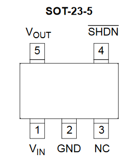
that put the GND pin squarely in the middle rather on the side of the component, I now find myself in the position of having no choice but to connect a trough-hole to GND by laying tracks right through the NC pin, since under the component laid several tiny trough-holes already.

So I'm wondering is it OK for me to do that (connect NC to GND)? Since in the datasheet it specifically said:

enter image description here

But I'm not 100% sure?

Or I could be wrong, there shouldn't be any non-GND via under the power IC, and instead, there should be a patch of GND plane?

\$\endgroup\$
7
  • 1
    \$\begingroup\$ LOL don't you just love English.... good question. By "no internal connection " you could assume do what you want... but "true No Connect" means the opposite. \$\endgroup\$
    – Trevor_G
    Commented Mar 22, 2017 at 1:55
  • \$\begingroup\$ So how am I supposed to interpret it? I shouldn't connect it to anything? \$\endgroup\$
    – Matt Cox
    Commented Mar 22, 2017 at 2:03
  • 1
    \$\begingroup\$ I'd like to say go with the No Internal Connection one and run your trace through there, but I won't. If you have one you can always test it and see if that is a problem just to be sure. \$\endgroup\$
    – Trevor_G
    Commented Mar 22, 2017 at 2:06
  • \$\begingroup\$ I'm confused by your PCB description though. Did you not use the recommended land pattern? \$\endgroup\$
    – Trevor_G
    Commented Mar 22, 2017 at 2:19
  • 2
    \$\begingroup\$ You have several options: 1. Use appropriate board tracing technology to route the part in accord with specifications, making your layout less brimful and more optimal; 2. Send e-mail to Microchip support and ask what is "true no connect" pin and if they approve the connection. 3. You can x-ray the part to determine if there is any bond wire on this particular batch of chips. However, "no internal connection" sounds pretty 100% definitive to me. \$\endgroup\$ Commented Mar 22, 2017 at 3:08

2 Answers 2

5
\$\begingroup\$

This one is really clear, surprisingly clear in fact ... downright enlightened. That additional wording that MicroChip put in ... "true ..." makes it a very safe bet that you can perform whatever routing function through that pin you wish to ease your layout. The only caveat is not to put a sensitive net through the pin, since it will add parasitics (a handful of pF) if it matters.

Alternate wordings would be "DNC" for do not connect, which is a command, not a suggestion. or "Reserved" where you must fear for your life if you ever connect that pin incorrectly.

I've been reading data sheets since the '70s and they have not been better or worse across time. This one is very clear.

To convince yourself, put your meter on the highest resistance range to each pin in turn. Checking that it declares over-range. Make sure that you perform each measurement with both polarities of the meter. Most meters use a one-polarity source, often ramping in a triangle, so they read differently each way and a diode will fool you.

\$\endgroup\$
19
  • \$\begingroup\$ The datasheet is very clear. "No internal connection. The pins marked NC are true “No Connect” pins". How is that NOT clear???? "it will add parasitics" How will it do that? No electrons will flow through it. It's going to add parasitics to Ground? How? Remember, there is NO INTERNAL CONNECTION, it is not connected to anything. Nowhere for electrons to go. \$\endgroup\$ Commented Mar 22, 2017 at 3:50
  • 1
    \$\begingroup\$ Well ... No internal connection means that there are no silicon connections to that pin, thus it is great for not hurting the device to connect as you please. As for parasitics, there are electrons flowing onto the tiny capacitor that the pin creates to the rest of the world. That parasitic won't upset this application, but if this were high speed or super low current, then it would upset the electrons on the board trace. \$\endgroup\$
    – catraeus
    Commented Mar 22, 2017 at 4:04
  • 1
    \$\begingroup\$ I have seen some cases where NC actually was intended to say DNC. Reading the datasheet (RTFM as they say) you find whether it has no internal connection or is meant to say that it is a must-not-connect. I double check most everything. I have designed pacemakers, there is no room for "oh well I'm sure that it actually means ... " \$\endgroup\$
    – catraeus
    Commented Mar 23, 2017 at 22:26
  • 1
    \$\begingroup\$ @Misunderstood on parasitic cap. It is from the metal surface of the pin ( it can go for a few mm inside the device on bigger chips) to all of the other circuit conductors that pass nearby. The electric field makes an air capacitor between the pin and other conductors. It is specific to the special cases I indicated. For example, that pin on this device we've been discussing would shut down DDR4 if it was used as a pass-through route. It doesn't do diddly to the 2A current that comes from the ground or power connections of this device. \$\endgroup\$
    – catraeus
    Commented Mar 23, 2017 at 22:29
  • 1
    \$\begingroup\$ @tangrs Electric current flow comes from two means. One is actual electrons (or protons) that physically move through space. The other, much more subtle concept, is that electric current flow is due to changing electric fields. Look up Displacement Current \$\endgroup\$
    – catraeus
    Commented Mar 23, 2017 at 22:32
0
\$\begingroup\$

NC or 'No connect' usually means 'Not connected', unless the datasheet says otherwise. DNC or 'DO NOT CONNECT' means do not connect for any reason. (and is could be a factor pin used for manufacturing, or other purposes)

\$\endgroup\$

Your Answer

By clicking “Post Your Answer”, you agree to our terms of service and acknowledge you have read our privacy policy.

Not the answer you're looking for? Browse other questions tagged or ask your own question.