4
\$\begingroup\$

This is something of a follow-up question to one I asked a few days back (Original JFET Hartley Question). Having made the changes suggested in the comments (i.e., changing Rd/R3 to 270 ohms, instead of 270k) and some basic biasing tweaks, I finally got the circuit oscillating on the board.

However, at the high end of the tuning range (around 2MHz), I noticed that the sine wave was distorted. Not grossly distorted, but it had flat tops and a slightly breaking wave shape. I felt the layout was adequate and I went looking for other problems with the circuit, turning to similar JFET designs (something I probably should have done at the start!)

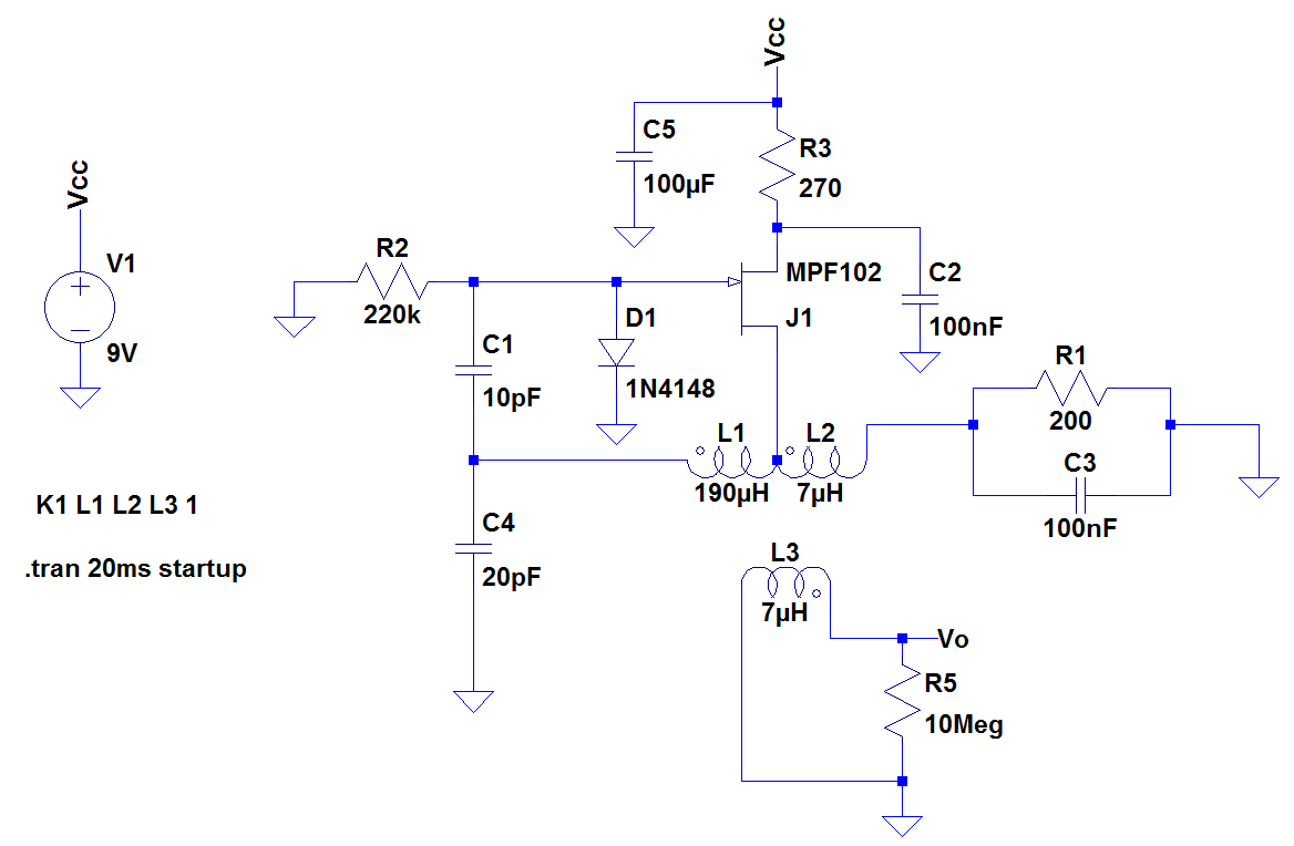
The modified circuit I came up with was the following:

enter image description here

The resulting sine wave was very good, with little distortion throughout the tuning range. But, the single most effective change was the introduction of D1 at the gate of the JFET. I haven't had much luck looking for a decent explanation as to why this diode makes a difference.

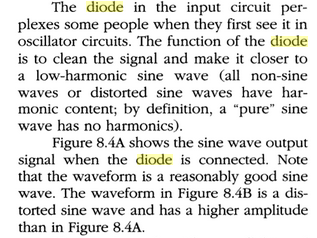
The best I could find was this snippet from J Carr:

enter image description here

All very fine, but how exactly does it "clean the signal"?

\$\endgroup\$
2
  • \$\begingroup\$ Loop gain may be too high. Try increasing R1. Or try decreasing C1. Or try an actual load R at Vo - with a small enough load, it'll quit oscillating. The AGC action of D1 can provide a more constant Vo for variations of load R. \$\endgroup\$
    – glen_geek
    Commented Apr 3, 2017 at 21:39
  • \$\begingroup\$ @glen it works like a charm at the moment probing Vo with a 10x probe. I'm planning to follow this stage with a JFET buffer, so no worries regarding load. Care to elaborate on the AGC action of D1? \$\endgroup\$
    – Buck8pe
    Commented Apr 3, 2017 at 21:49

4 Answers 4

4
\$\begingroup\$

It looks to me that the diode is there to shift the DC level of the signal coupled to the gate so that the positive peaks are just one diode drop above ground. That makes the negative peaks lower than they would be if the signal was centered around ground. Note that the signal is capacitively coupled to the gate. This is a JFET, so negative gate signals are meaningful.

The description you cite looks like nonsense. The overall effect of the diode may be to reduce harmonic content of the resulting oscillations, but the diode itself doesn't somehow magically "clean" the signal. By lowering the DC level of the signal on the gate, it's possible that the FET is operated in its linear region more, which would reduce the resulting harmonic content. But, that's far from the diode "cleaning" the signal. At best you can say the diode shifts the DC so that the FET can handle the signal more cleanly.

\$\endgroup\$
6
  • 3
    \$\begingroup\$ By raising the DC level of the signal on the gate I think the DC level (middle of the sine wave) is actually lowered since the diode clamps the top of the sinewave to +0.7 V. Lowering the DC biasing at the gate makes sense to me as the linear region of a JFET is for a negative Vgs. \$\endgroup\$ Commented Apr 3, 2017 at 20:51
  • \$\begingroup\$ @FakeMoustache I think you're right. I doubled checked the spice sim and the signal voltage is clipped at ~.7V and extends down to -14V. \$\endgroup\$
    – Buck8pe
    Commented Apr 3, 2017 at 20:53
  • \$\begingroup\$ Is that it then? It simply lowers the DC bias? I thought that maybe the non-linear action of the diode itself had some effect. \$\endgroup\$
    – Buck8pe
    Commented Apr 3, 2017 at 21:00
  • \$\begingroup\$ @Fake: Oops. Fixed. The reason that a mostly negative gate voltage is useful is because this is a JFET. \$\endgroup\$ Commented Apr 3, 2017 at 21:03
  • 1
    \$\begingroup\$ why can't you adjust the DC bias using R1? You can, but only partly. Looking at the transformer ratios I think there is a (much) larger signal swing at the gate than there is at the source. The DC-shift we want to make at the gate (to keep Vgs mainly negative) is more than we can achieve with the value of R1. Also increasing the value of R1 lowers the Ids which lowers gm so the loopgain is lowered. Lower R1 too much and the oscillator will not work due to lack of loopgain. \$\endgroup\$ Commented Apr 4, 2017 at 5:54
2
\$\begingroup\$

In any linear oscillator design you need to ensure that the gain is not much more than necessary for the oscillation to start. Ideally you would have a loop gain of 1, but in reality you need a loop gain slightly larger than 1 to account for component variability. That is a non-stable exponentially growing oscillation condition, that has to be limited somehow.

To achieve this, all linear oscillator designs rely on some level of nonlinearity to ensure that the loop gain is reduced to slightly below 1 at the desired output amplitude, this is normally a smooth reduction to avoid introducing too much distortion. The placement of this non-linearity is what defines the output amplitude. If the loop gain is much more than 1 the sine wave will flatten out as the energy in the storage elements, due to the excessive loop gain, will end up overdriving the input.

In that design, as you increase the frequency, C1 couples more and more of the output into the input of the amplifier, thus increasing loop gain. That is why you see distortions without the diode. You could have reduced the distortion at higher frequencies just by reducing C1, but then it would not oscillate at lower frequencies.

The diode, by conducting at the positive peaks of the signal does two things:

  1. It clips the maximum positive "bias" of the JFET, ensuring that the overall current is reduced, and thus limiting the amplifier gain.
  2. It presents a non-linear resistance to ground, creating a voltage divider with C1 which reduces the feedback gain at higher frequencies.
\$\endgroup\$
0
\$\begingroup\$

According to this video The Hartley and Colpitts Oscillators with Demo (AD# 103) the diode is there to limit feedback.

\$\endgroup\$
2
  • \$\begingroup\$ Link-only answers are not generally well-liked here; answers should be self-contained and not rely on external links. \$\endgroup\$
    – Hearth
    Commented Dec 4, 2018 at 3:01
  • \$\begingroup\$ I did explain what the diode was for and added a citation which is just good practice, I suggest you look at Wikipedia for other examples where people give justification of their answers. I am sorry I bothered now. \$\endgroup\$
    – mikee
    Commented Dec 5, 2018 at 15:49
0
\$\begingroup\$

The diode will cause the source voltage to go negative which reduces the overall gain to 'just enough' to keep it oscillating and thus reduce harmonic content. I have seen this reduce the third harmonic on an xtal oscillator by over 40 dB!

\$\endgroup\$

Your Answer

By clicking “Post Your Answer”, you agree to our terms of service and acknowledge you have read our privacy policy.

Not the answer you're looking for? Browse other questions tagged or ask your own question.