0
\$\begingroup\$

I am diagnosing a legacy design that uses an AD7862 SAR ADC.

  • Input is 500 Hz, 2.4 Vpp sinusoid, relatively low noise.
  • Digitized output adds a noise component waveform +/- ca 0.25 Vpp.
  • The FFT spectral peak (7484 Hz) of the noise is close to the sample rate, 7782 Hz. I expect a small amount of sample rate noise, but not this extreme amount. The noise waveform appears sinusoidal as well, not as a typical quantization.
  • Of course I can FIR it after the fact, but would rather find root cause.
  • The digital control signals to ADC are ringing to the point where they almost reach V(INH) and V(INL) thresholds. Could be false triggering? Affecting the SAR process? Otherwise digital signals are nominal.
  • Happy to share diagrams, etc.
\$\endgroup\$
4
  • \$\begingroup\$ What is the sample rate then? A signal at the sample rate is the same as DC so cannot be resolved in the FFT. \$\endgroup\$ Commented Apr 6, 2017 at 17:23
  • \$\begingroup\$ The most likely cause of the ringing on the digital signals is poor probing technique, especially the scope ground - make it SHORT. \$\endgroup\$ Commented Apr 6, 2017 at 17:24
  • \$\begingroup\$ You sure the sample rate isn't 8000 Hz and you're seeing 500 Hz aliased at 8000-500 = 7500 Hz? \$\endgroup\$ Commented Apr 6, 2017 at 17:54
  • \$\begingroup\$ The FFT is 2048 point, the most this system can handle. The noise peak is at 7484 Hz, but this has a large tolerance on it. The /CONVST pulses occur at 7782 Hz. And again, it is possible that digital control signals are ringing excessively, thus thwarting normal timing requirements. The impressed noise does not look at all like a digitization effect. It is itself very sinusoidal. Probe is 600 MHz, grounded within 1 cm of test node. Scope is 600 MHz, 5 GSa/s. That's not the problem. \$\endgroup\$ Commented Apr 6, 2017 at 18:27

1 Answer 1

0
\$\begingroup\$

Interface Noise, from the digital side, can set a floor, as you have seen. Cure?

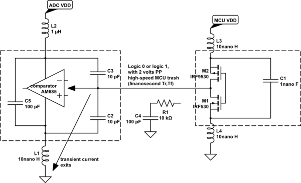
The MCU rings, because 1nanosecond clock-charge surges abruptly discharge the onchip charge-bucket, the various parasitic well-substrate capacitors and any unused FET gates in the quiescent logic/flops/memories. This abrupt sag of VDD (and rise of GND) in the MCU will appear on the interface signals to the ADC. Ringing will be approximately 100MHz, perhaps 200MHz. We'll use 100MHz at +-1volt. The slewrate is d(1*sin(100MHz*2pi*t))/dt = 628 MegaVolts.

All your interfaces signals, even "quiet" levels, will have this trash and this slewrate.

Your ADC ESD structures, between 3pF and 10pF in size, response to these changing voltages, and currents flow; those currents need to return home, back to the MCU, and those currents explore all possible paths, including out the analog signal inputs from your sensor. Most of the current goes out the lowest impedance path, the ADC VDD and GND, thru those inductances. Those inductances ring because of the onchip well-substrate capacitances.

schematic

simulate this circuit – Schematic created using CircuitLab

Solution? slow down the edges and reduce the amplitude of the currents. How? insert resistors (1k or 10K) in the interface lines, and add 100pF caps at the ADC side of the interfaces.

\$\endgroup\$

Your Answer

By clicking “Post Your Answer”, you agree to our terms of service and acknowledge you have read our privacy policy.

Not the answer you're looking for? Browse other questions tagged or ask your own question.