0
\$\begingroup\$

I am trying to build an Arduino version of the voltammetry thing described in this paper. Before questions here is a little background for those who don't know what voltammetry is.

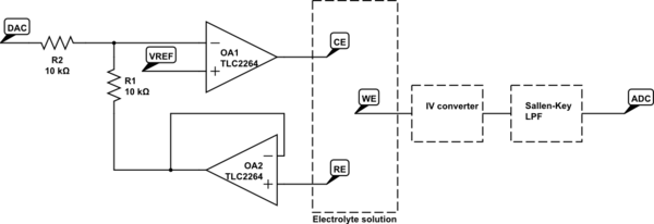
This device works with three electrodes, working electrode (WE), counter electrode (CE), reference electrode (RE), immersed in a solution (containing the sample and electrolytes). A potential (fixed, linearly increasing or cyclic) is applied between CE and WE, and if high enough, redox processes happen on these electrodes and some current flows between them. The reference electrode is there to provide a fixed V reference. The device must measure the current flowing from CE to WE and the voltage between RE an WE in order to build a voltammogram (x=V, y=I).

Here a simplified version of the schematics:
schematic

simulate this circuit – Schematic created using CircuitLab

The original project use an Atmel XMEGA. Vref is internal 1V. Op amp single supply is 5V.

  • How does that feedback work? Hint: when DAC put out, for example, 2V referred to ground, the opamp must put out 2V between CE and RE. No current must flow through RE.
  • Arduino does not have a DAC, can I build a low pass PWM filter on top of the first op amp or it is better to have two RC filters before it?

EDIT

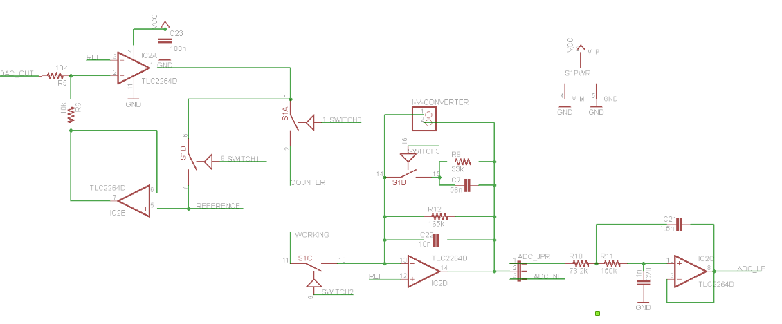
Added original schematics

(Note: S1D is open during operation while S1A and S1C are closed, those switches are for dry tests)

enter image description here

\$\endgroup\$
0

2 Answers 2

0
\$\begingroup\$

As shown , OA1 has a DAC gain of -1 and the Vref puts 2V out on CE (OA1 out) plus any additional voltage to overcome the current drawn by WE such that OA2in is always 2x Vref=2V.

Thus there is zero current thru CE & RE but with infinite impedance across the electrolyte, even if a cell potential is inserted.

However sensor electrode WE picks up the difference between CE*RE or 2x Vref and 2xVref-DAC and any current drawn to some high impedance load to ground is detected as a voltage or current converted to a voltage with 0V reference.

If located in the middle, the DAC potential will be divided by 2 including Vref*2. (thus 1Vdc)

However I do not see the need for current voltage conversion as it is driven by a voltage source instead of a current source which is more conventional for impedance spectroscopy with DC bias.

\$\endgroup\$
4
  • \$\begingroup\$ Thanks, things starts to clear up! but I don't know if I got the last part. I don't think this is impedance spectroscopy, electrons actually develop from the solution due to redox reactions, I have to detect a current, hence the IV converter. I have added the original schematics to the question. \$\endgroup\$
    – user288431
    Commented Apr 9, 2017 at 22:55
  • \$\begingroup\$ OK so no AC, just DC. It's not how I would do this. I would drive with a Constant current source and measure voltage which is now proportional to impedance. \$\endgroup\$
    – D.A.S.
    Commented Apr 9, 2017 at 22:59
  • \$\begingroup\$ yes yes AC, but since the voltage are shifted the opamps (and DAC) always work in positive values, with VREF as 0. The ADC is configured to read values that are less then VREF as negative \$\endgroup\$
    – user288431
    Commented Apr 9, 2017 at 23:02
  • \$\begingroup\$ The solution (between CE and WE) must "perceive" an AC with V(RE) as 0, usually with a max swing of +- 1 to not destroy the electrodes \$\endgroup\$
    – user288431
    Commented Apr 9, 2017 at 23:02
0
\$\begingroup\$
  1. My "knee-jerk reaction" to this circuit is "those poor, melted Op-Amps! While on closer inspection, the circuit looks (at least potentially) feasible, any delay-time between voltage changes in CE and the corresponding voltage potential change at RE would likely lead to oscillations & likely catastrophic destruction of the Op Amps, IMHO.

  2. OA2 is operating as a simple "voltage follower" or "buffer amp." Its function is to take virtually no current from RE, while "reading" it's voltage, then output the same voltage with a low impedance (high current), to feed into the resistor network for OA1's inverting input.
    OA1 is functioning as a comparator, with the "feedback" from OA2 mixing with the "input" from your DAC being "compared" to your reference voltage (+1V).
    On the inverting input, both DAC "input" and OA1 "feedback" pass through equal-value resistors, so the voltage detected on the inverting input should be "half-way between" the 2 values (i.e. if DAC is outputting 2V, and RE is at 0V, then 1V should be sensed, or if DAC is at 2V & RE at 1V, then 1.5V sensed). Whenever OA1 senses a higher input from DAC+OA2 than Vref, its output will swing low, and whenever Vref>DAC+OA2, its output will swing high.
    In theory, the voltage applied to CE should reach RE fast enough that the output of OA2 will either look like a PWM waveform, or (if OA2 has a low enough slew rate) will have lower-amplitude oscillations, "seeking" a voltage output that satisfies the equation (RE+DAC)/2=Vref.
    In practice, I'd make sure to use an OA2 with a LOW slew rate, in order to reduce the likelihood of having it "hit the rails" when oscillating PWM-style & potentially cause the Op Amp to "latch up" to one of its two supply rails, and cease operating correctly.

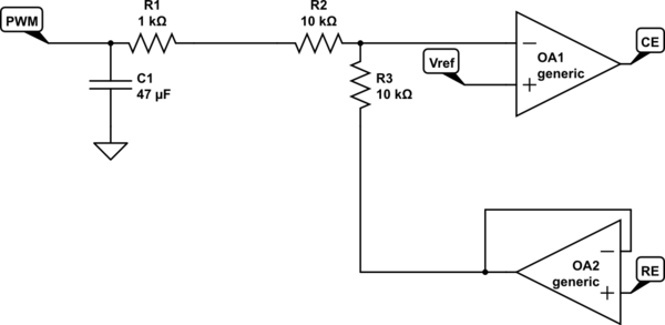
  3. You should be fine using PWM for your DAC, just make sure to put your LPF (RC works well) before the 10k resistor that's between positions DAC & OA2 inverting input on the diagram, like this:

schematic

simulate this circuit – Schematic created using CircuitLab

Ideally, you may want to connect an ADC pin from between the 1K & 10K resistors, so the 'duino can detect the actual PWM voltage output it's feeding into the circuit, if this is an important parameter.

\$\endgroup\$

Your Answer

By clicking “Post Your Answer”, you agree to our terms of service and acknowledge you have read our privacy policy.

Not the answer you're looking for? Browse other questions tagged or ask your own question.