1
\$\begingroup\$

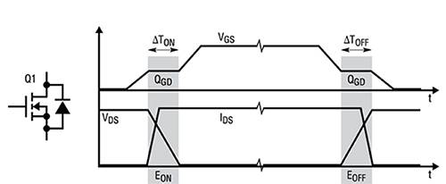
I am currently trying to build conventional bi-directional DC converter and see the mosfet behavior when controlled with PWM signal. based on theory, the drain-source current (Ids) and drain to source voltage (Vds) will switch at the same times when the mosfet turned on or off as illustrated in figure 1. this known as hard switching. but when i tested in actual bi-converter that i made, the waveform of Ids is somehow different from what i expected (far from trapezoidal waveform). As you can see in Figure 2, the Ids is somehow take a long time to rise and fall even the gate already switched.

Figure 1. Switching Waveform on Mosfet

Figure 1

Figure 2. My Actual Switching Waveform on Mosfet, yellow (Vds), Blue (Ids), Magenta (Vgs)

Figure 2

I am quite new to electronic, and what I've been doing so far are

  1. Made Conventional Bi-DC Converter. the mosfet behavior is in figure 2.
  2. adding capacitor paralleled with drain pin and source pin on mosfet. this capacitor affect on Vds.
  3. the voltage observed with passive oscilloscope probe; and current observed with clamp probe (not stable waveform) then switched to differential probe (more stable waveform).

what I want to ask are:

  1. is there any possible explanation of this mosfet Ids waveform behavior?
  2. what can I do to make the Ids waveform on mosfet more trapezoidal (close to ideal hard switching waveform)?

I knew that hard-switching is not good, but i need to generate hard switching waveform in actual converter i made for my project. anyone with more experience with this Please help me, thanks.

EDIT: This is my converter schematic. figure 2 generated under buck mode.

Ids, Vds and Vgs tested on S1 switch.
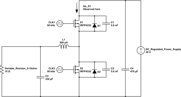
schematic

simulate this circuit – Schematic created using CircuitLab

Input: 0-30 Volt DC regulated power supply.

Load : variable resistor 0-10 ohm.

Switch: Mosfet IRFP4332

www.infineon.com/dgdl/irfp4332pbf.pdf?fileId=5546d462533600a40153562c58682013

Mosfet Driver circuit based on this blog: TLP250 Mosfet Driver Circuit

tahmidmc.blogspot.co.id/2013/05/using-tlp250-for-isolated-mosfet-gate.html

\$\endgroup\$
10
  • 2
    \$\begingroup\$ You are obviously driving an inductive load, or have a significant inductance somewhere in the power line. As such the current can not instantaneously change. \$\endgroup\$
    – Trevor_G
    Commented Apr 11, 2017 at 2:36
  • \$\begingroup\$ Can you add whole schematic of your circuit? \$\endgroup\$ Commented Apr 11, 2017 at 4:17
  • \$\begingroup\$ Show the exact circuit and explain what load you are driving. \$\endgroup\$
    – Andy aka
    Commented Apr 11, 2017 at 8:30
  • 2
    \$\begingroup\$ @Dian Akbar: have you ever seen this formular: v = L di/dt? Solved for di/dt yields di/dt = v/L = 30V / 200µH = 0.15 A/µs. This is the max. rate of current change you can expect. \$\endgroup\$
    – Curd
    Commented Apr 11, 2017 at 10:22
  • 1
    \$\begingroup\$ @Dian Akbar: What do you mean by "will only applied to I_L1"? Of course it affects only I_L1 but I_L1 is the same as I_DS (of either MOSFET) as there is no other current path through the MOSFETs except the one from L (unless you are turning on both MOSFETs at the same time which would be stupid). Also note that I was talking about max. di/dt. I.e. there are still other factors that affect the voltage across L and thus di/dt, e.g. ESR of inductor, Ron of MOSFET or your "variable resistor", etc. \$\endgroup\$
    – Curd
    Commented Apr 12, 2017 at 19:18

1 Answer 1

1
\$\begingroup\$

@Andyaka detail Added. I use resistive load only for the load

I beg to differ, clearly there is a 200 uH inductor in series with the output as would be the case in many designs (but different values).

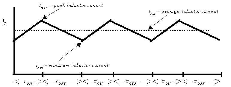
This is the item that causes the slow rise and fall times of current through the drain of the MOSFET. This is the sort of waveform you should see: -

enter image description here

And, if your switching frequency is lowered you will see start to compress at the peaks (as is seen in your picture).

V = L di/dt or, rearranged, if you put a constant voltage across an inductor of value L you get a constant value of di/dt (rising or falling).

\$\endgroup\$
3
  • \$\begingroup\$ thankyou for answering. Based on your explanation, the waveform you give will appear exactly like that if I probed on L1, but I checked on I_ds instead of L1. based on simulation, the waveform in Ids will only match the charging state of L1 when mosfet on t_on, and will go to zero when mosfet t_off. the Ids on my mosfet appear to be overdamped with slow rise time. I think there must be some correlation with mosfet specification, with what affecting the di/dt of mosfet, with how to choose mosfet with fast current transient recovery. \$\endgroup\$
    – Dian Akbar
    Commented Apr 12, 2017 at 15:40
  • \$\begingroup\$ I also checked the waveform when using different value of Inductor with my actual converter. the changes did not make the mosfet current Ids appear more instantaneous. \$\endgroup\$
    – Dian Akbar
    Commented Apr 12, 2017 at 15:45
  • \$\begingroup\$ @DianAkbar "if I probes on L1". It still seems you don't gasp the concept of KCL. Inductor current = MOSFET current unless you have cross conduction. \$\endgroup\$
    – winny
    Commented May 14, 2017 at 9:08

Your Answer

By clicking “Post Your Answer”, you agree to our terms of service and acknowledge you have read our privacy policy.

Not the answer you're looking for? Browse other questions tagged or ask your own question.