1
\$\begingroup\$

enter image description here

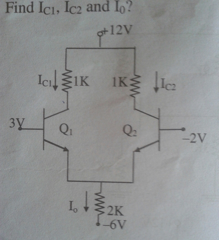
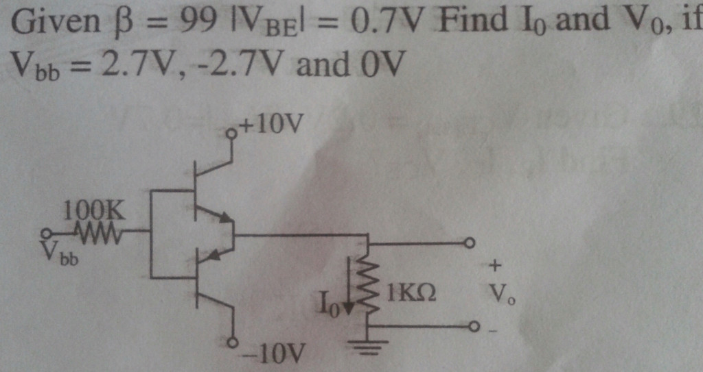
here in this question's solution, given that upper BJT is on while lower one is in cutoff region for Vbb = 2.7 V and viceversa for Vbb = -2.7 V and both will be in cutoff for 0 V. While in other problem Q1 is on and Q2 is in cutoff.

So my question is how to decide which one will be conducting and which one will be off and why? Is there any general procedure?

\$\endgroup\$
4
  • \$\begingroup\$ What is needed to turn on an NPN transistor? What is needed to turn on a PNP transistor? \$\endgroup\$ Commented Apr 17, 2017 at 11:36
  • \$\begingroup\$ You mean transistors not thyristors \$\endgroup\$
    – user16222
    Commented Apr 17, 2017 at 12:29
  • \$\begingroup\$ Look at where your load, the \$1\:\textrm{k}\Omega\$ resistor, is connected. Ground, right? So, knowing that the load only has direct access to ground, can you tell which BJT will be ON when \$V_{bb}\$ is positive, is negative, and is zero (relative to ground)? I think this is a case where first looking at the load helps a lot more than getting mired in worrying over the rest, too early. \$\endgroup\$
    – jonk
    Commented Apr 17, 2017 at 17:17
  • \$\begingroup\$ Yes your hint works but only in this particular problem but how to approach when load is connected to negative source i have one example like that (see another image) \$\endgroup\$
    – user146551
    Commented Apr 18, 2017 at 1:30

3 Answers 3

1
\$\begingroup\$

Look at this circuit carefully and realize each transistor is being used in emitter follower mode. However, as you say, at most one of them is on at a time.

To decide whether a transistor is on or off, look at the voltage across its B-E junction.

Hint: Remove any transistor that is off from the circuit, then analyze.

\$\endgroup\$
1
  • \$\begingroup\$ Ah, you beat me to it, had this typed in when yours appeared :-) Spot on. \$\endgroup\$
    – TonyM
    Commented Apr 17, 2017 at 12:37
0
\$\begingroup\$

Your two questions are not complicated. I suspect you are imagining they are worse than they really are. Let's apply simple logic with the more recently added schematic:
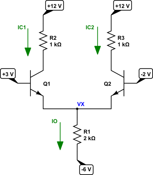
schematic

simulate this circuit – Schematic created using CircuitLab

First thing to do is to decide what the two transistors are doing. Suppose that \$Q_2\$'s \$V_{BE_2}\approx 700\:\textrm{mV}\$ and that it is therefore actively on. Then it follows that \$V_X\approx -2.7\:\textrm{V}\$. But if that were the case, then \$Q_1\$'s \$V_{BE_1}\approx 5.7\:\textrm{V}\$! Given that the collector current goes up by a factor of about 10 for each \$60\:\textrm{mV}\$, this would imply a HUGE collector current and probably a huge base current in \$Q_1\$. Not to mention that \$R_1\$ couldn't allow it, anyway.

Given that the two emitters share the same node, it's much more likely now that these details are exposed that \$Q_2\$ is actually off and \$Q_1\$ is the only transistor in an active mode. Once you realize this, you then know that \$V_X\approx 2.3\:\textrm{V}\$, that \$Q_2\$ is off, \$I_O=\frac{+2.3\:\textrm{V}- \left(-6\:\textrm{V}\right)}{2\:\textrm{k}\Omega}=4.15\:\textrm{mA}\$, \$I_{C_1}\approx 4.15\:\textrm{mA}\$ (slightly less than the emitter current because of a tiny base current), and that \$I_{C_2}\approx 0\:\textrm{mA}\$.

Another way to see that fact is to simply imagine the two transistors as both being completely off to start, and to then gradually activate \$R_1\$ by slowly pulling the \$-6\:\textrm{V}\$ rail downward, starting at the highest base voltage of \$+3\:\textrm{V}\$ and ramping it downward towards \$-6\:\textrm{V}\$ just a little bit at a time. Note that as you do this mental step, \$Q_1\$ will definitely be the first BJT to turn on. And once it turns on at around \$600\:\textrm{mV}\$ or so, when the bottom supply rail has only just reached about \$+2.4\:\textrm{V}\$, the emitter current will start rising upward by factors of 10 for each additional \$60\:\textrm{mV}\$ lower. It doesn't take much to then realize that the emitter of \$Q_1\$ will never allow the base-emitter junction of \$Q_2\$ to become forward biased. It just can't happen. So \$Q_2\$ is off. End of story.


Now you should be able to apply similar logic in your original case.

\$\endgroup\$
4
  • \$\begingroup\$ Are you saying that one with most positive Vb - Ve (for NPN) and most positive Ve - Vb (for PNP) will be on first and considering one of them on check for others Vbe (is it more than 0.7 V or not) \$\endgroup\$
    – user146551
    Commented Apr 24, 2017 at 5:44
  • \$\begingroup\$ @user146551 I can't parse your writing well. I apologize for that. What I am saying is that the magnitude, \$\vert V_{BE}\vert\$, can't get to much more than a volt because of the extremely large currents that implies. Every \$60\:\textrm{mV}\$ increase means 10 times the collector current. As the base-emitter voltage adds a little at a time, the collector current multiplies by large factors. This behavior causes one BJT to simply "take over" in the cases you show. \$\endgroup\$
    – jonk
    Commented Apr 24, 2017 at 6:15
  • \$\begingroup\$ I am trying to say that transistor with most positive Vbe will on first, considering it on we will check for other transistors Vbe if it will >0.7 volt then it will on too. \$\endgroup\$
    – user146551
    Commented Apr 24, 2017 at 6:21
  • \$\begingroup\$ @user146551 That works in your first schematic's case. The way I wrote about the issue is more general and will work in schematics that look more complex. Also, if the base voltages were a lot closer to each other in your first schematic, then the way you write probably wouldn't be useful anymore. But the way I write it still would be. For example, suppose the -2 V base were changed so that it was instead +2.94 V. Then both BJTs would be on, but the left one may have almost 10 times the collector current. Which would be important to know, sometimes. But whatever works. \$\endgroup\$
    – jonk
    Commented Apr 24, 2017 at 6:47
0
\$\begingroup\$

In cut off mode both junction of bjt (emitter-base and collector-base) will be in reverse biased condition. It can happen only if base is biased negatively (in NPN transistor) and biased positively in (PNP transistor).

\$\endgroup\$

Your Answer

By clicking “Post Your Answer”, you agree to our terms of service and acknowledge you have read our privacy policy.

Not the answer you're looking for? Browse other questions tagged or ask your own question.