1
\$\begingroup\$

I am designing a low-pass filter for a charge output transducer. The filter must be passive and provide a 2nd order Butterworth response, no more than 0.01dB of ripple in the passband is acceptable.

I have a filter available that does not meet my cutoff frequency requirements, but, as it operates on charge I am not sure how to approach analyzing or redesigning it.

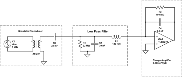
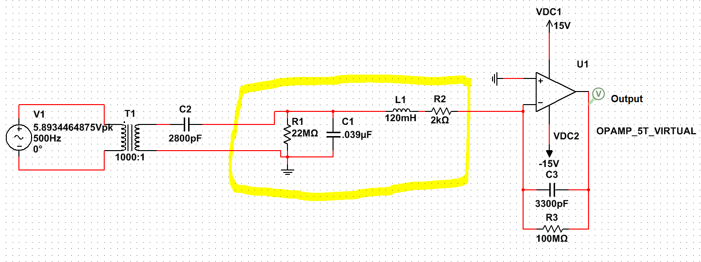
The attached image shows a model that I built to simulate the filter. The design shown gives an approximately 3 kHz cutoff.

  • The transducer is simulated by the voltage source, transformer and series capacitor.
  • An example of the lowpass filter topology is shown at the output of the simulated charge source.
  • A textbook charge amplifier has been included at the filter output (the choice of op-amp might not be ideal here).
schematic

simulate this circuit – Schematic created using CircuitLab

Schematic as Image

Can anyone offer insight into the design and analysis of the filter topology shown? Specifically, I would like to understand what method could be used to select the components to achieve a Butterworth response.

EDIT: The ripple and filter type requirements could be modified. The biggest challenge( for me at least) is designing a filter for charge signals. I am not sure how to use any standard technique to design such a filter.

\$\endgroup\$
3
  • \$\begingroup\$ I suggest the charge amp first and then the low pass filter afterward. The charge amplifier is an integrator, and constitutes somewhat of a low pass filter all by itself. \$\endgroup\$ Commented May 12, 2017 at 20:23
  • \$\begingroup\$ You never see anything between the piezo element and the amplifier in any application note I've ever seen. \$\endgroup\$ Commented May 12, 2017 at 20:24
  • \$\begingroup\$ I don't understand your simulation circuit, especially why you chose for a transformer. Also, most charge output elements are simulated by a current source parallel to a capacitor, in your case 2.8nF. Now look at what the 28 nF filter capacitor does: it attenuates your information containing signal by a factor 10! And on top of it the 22MOhm resistor will add noise. Not good at all, so at all means do consider a charge amplifier with higher supply voltage/dynamic range and do the filtering at the output of that. Also the higher frequencies you state are not reflected in the simulation. \$\endgroup\$
    – HarryH
    Commented Jun 13, 2019 at 21:57

2 Answers 2

1
\$\begingroup\$

Protect your signal integrity by capturing the charge on the feedback cap as early as you can. I suggest the charge amp first and then the low pass filter afterward. The charge amplifier is an integrator, and constitutes somewhat of a low pass filter all by itself.

I've never seen anything between the piezo element and the amplifier in any application note I've ever seen.

If you must filter, filter later, unless you can think of a very solid reason why you need to do otherwise

\$\endgroup\$
3
  • \$\begingroup\$ The people who make charge amps make inline pre filters. The lead times are horrendous, so, I need to build something. In my application the high-frequency signal content is too large and causes the amplifier to saturate. The amplifiers are commercial products and cannot be replaced or modified. I'm really hoping someone could offer advice on designing a charge mode filter. \$\endgroup\$ Commented May 12, 2017 at 21:01
  • \$\begingroup\$ I see you point, but what about selecting an amplifier that doesn't saturate on the high-frequency content? \$\endgroup\$
    – HarryH
    Commented Jun 13, 2019 at 21:53
  • \$\begingroup\$ Sorry, I missed the point 'cannot be replaced'. However, you seem to have space to insert filters, wouldn't it be possible to just bypass the 'commercial products' and insert your own high dynamic range charge amplifier followed by a filter while leaving the 'commercial products' in place? \$\endgroup\$
    – HarryH
    Commented Jun 13, 2019 at 22:02
0
\$\begingroup\$

While speaking about "0.01 dB ripple" in the passband - are you aware that this requirement does specify your cutoff frequency? What is the passband required? And what about using another filter topology?

\$\endgroup\$
3
  • \$\begingroup\$ The LP cutoff frequency should be ~2kHz, some variation in the performance will be inevitable due to uncertainty in the transducer and cable source capacitance. It is also a requirement to maintain the source capacitance presented to the charge converter below 15nF. Changing the topology is acceptable, provided it remains suitable for the application of filtering a charge signal. \$\endgroup\$ Commented May 12, 2017 at 15:48
  • \$\begingroup\$ To be clear: Just 0.01 dB ripple allowed between 0 and 2kHz - right? Why not using a standard Chebyshev response (0.01dB) ? \$\endgroup\$
    – LvW
    Commented May 12, 2017 at 18:22
  • \$\begingroup\$ The ripple and filter type requirements could be modified. The biggest challenge( for me at least) is designing a filter for charge signals. I am not sure how to use any standard technique to design such a filter. \$\endgroup\$ Commented May 12, 2017 at 19:51

Your Answer

By clicking “Post Your Answer”, you agree to our terms of service and acknowledge you have read our privacy policy.

Not the answer you're looking for? Browse other questions tagged or ask your own question.