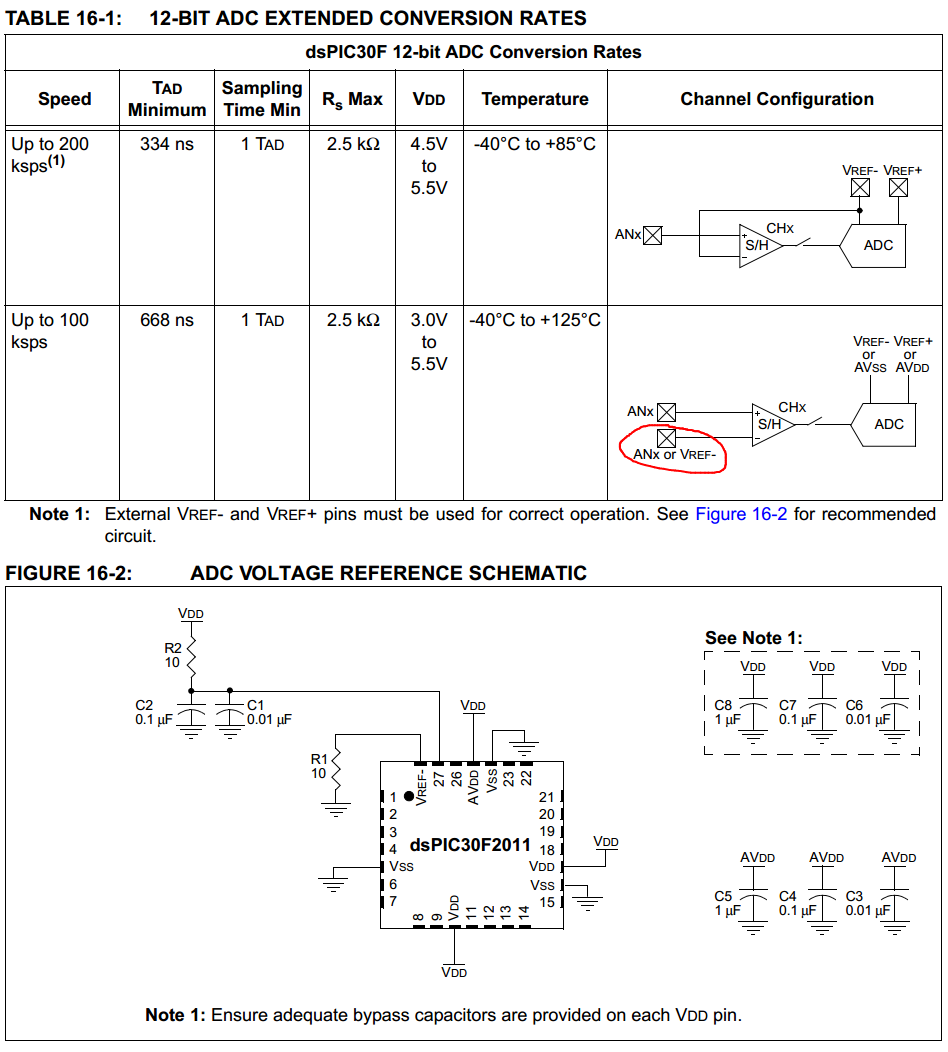
While trying to get the ADC of the dsPICF3013 working (I am getting only zeros back), I have studied the datasheet and the (I will call it) ADC reference for the dsPIC30F family. Previously I only worked with the ADC of the PIC16F, so now I have to face a lot of more options.
The ADC is configured to use \$AV_{DD}\$ as the positive voltage reference and \$AV_{SS}\$ as the negative voltage reference. The ADCON2.VCFG<2:0> configuration bits are set to 000 (see page 18-6 of the ADC reference). As I understand it the \$V_{REF-}\$ and \$V_{REF+}\$ pins are now available for general use (although I did not find it documented explicitly).
But taking a look at Table 16-1 and Figure 16-2 on page 116 in the datasheet, it looks like the \$V_{REF-}\$ and \$V_{REF+}\$ pins always have to be connected. Especially the diagram in Table 16-1 confuses me (I marked it red. Shouldn't I be able to connect it to \$AV_{SS}\$?).

The first part of my question: Do I always have to connect the \$V_{REF-}\$ and/or \$V_{REF+}\$ pins or can they be turned into general purpose pins?
The second part of my question refers to the ADCHS.CH0NA configuration bit on page 18-8 in the ADC reference. Here I can set the negative input (=negative voltage reference?) to the ADC: AN1 or \$V_{REF-}\$. AN1 is obviously a pin. But what about \$V_{REF-}\$? They map both to the same physical pin. Does \$V_{REF-}\$ in this case refer to the settings of the ADCON2.VCFG<2:0> configuration bits or to the actual pin (that wouldn't make sense at all)?
I ask this second question, because in table Table 16-1 I mentioned above they (\$V_{REF-}\$ as negative voltage reference vs actual pin name) are not the same.
