0
\$\begingroup\$

Currently, I am using a function generator to drive MOSFET with a 5V square wave. Now I need to rise frequency up to 14 MHz for educational purposes. Before I post an order for specific IC, I want to consult with more experienced people. This is my first time using a mos driver.

So, I need to drive only one fet. I found this driver

The datasheet states: Wide Input Supply Voltage Operating Range: -4.5V to 18V.
But later it reads, in Absolute Maximum Ratings: Input Voltage –5V to VDD + 0.3V So wich is it,? As input, I consider a signal from a function generator, correct?

Also, on pin 1 and 8 is Vdd. I am guessing pin1 is for powering a chip and pin 8 for driving MOSFET. Correct me if I am wrong.

Matched Rise and Fall Times: 25 ns. Does it mean operating frequency of 50ns which is 20MHz?

Last question, if I feed input with 5V does the output equals input 5V or Vdd from pin8?

\$\endgroup\$
3
  • 2
    \$\begingroup\$ This driver has rise+fall times = 70ns. 14Mhz frequncy has a period of 71.4ns. Also the propagation delays between input and output are 70ns+70ns, which is twice your period. This driver is not suitable for such frequency. I don't even want to imagine what output it will give. 14Mhz is a very high frequency for a MOSFET driver. \$\endgroup\$ Commented May 25, 2017 at 20:24
  • \$\begingroup\$ MAx on the chart Figure 2.9 is 4MHz, after that it will just cook. It might up there anyway.... since it will only be half on most of the time \$\endgroup\$
    – Trevor_G
    Commented May 25, 2017 at 20:25
  • \$\begingroup\$ The real question is: what kind of MOSFET are trying to drive at 14MHz, and for what reason? \$\endgroup\$ Commented May 25, 2017 at 20:53

2 Answers 2

1
\$\begingroup\$
  1. You've read the "Wide Input Supply Voltage Operating Range" incorrectly. The range is from +4.5V to +18V for normal operations.
  2. "Absolute Maximum Ratings" refers to what voltages will not damage the device. "Input Voltage" is referring to the voltage at the Input pin, not the main power input VDD. It is saying that even accidentally applying negative 5V, up to 0.3V above your main supply voltage (VDD), to the Input pin will not hurt the device.
  3. When chips label multiple pins as the same name, they always mean they are internally electrically connected, unless they very explicitly state otherwise. In this case, they have provided two terminals to get power into the device because the losses associated with using only a single pin would be higher. They have also provided two pins for the output current for the same reason. In general, always connect all internally connected pins to each other externally. However, if you need to cut corners for other reasons, things generally still work if you don't connect all of the pins.
  4. Yes, because the rise & fall times are 25ns, if you used an operative frequency of 20MHz (a period of 50ns) and 50% duty cycle, the output FETs would basically never turn on. You would just dump a bunch of energy (aka heat) into the FET gates and the load would basically never turn on. Running at 14Mhz will get very close to this and you might overheat and blow up your FETs.
  5. Output will be tied to either VDD or GND, depending on the state of Input. Therefore, when Input is at 5V, relative to GND, Output will be connected to VDD.
\$\endgroup\$
0
\$\begingroup\$

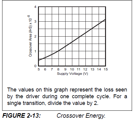
Power is consumed during output swings, during which times BOTH output MOSFETs are on and crowbarring the 18 volt rail;

enter image description here

At 18 volts, this internal heating is 18 volts * 4 e-8 Amp*seconds or 72 e-8 joules, or 0.72 microJoules. At 14MHz, this internal selfheating is exactly 10 watt. Is this a dual driver? Does the thermal resistance tolerate 10 watt heating?

\$\endgroup\$

Your Answer

By clicking “Post Your Answer”, you agree to our terms of service and acknowledge you have read our privacy policy.

Not the answer you're looking for? Browse other questions tagged or ask your own question.