0
\$\begingroup\$

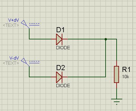
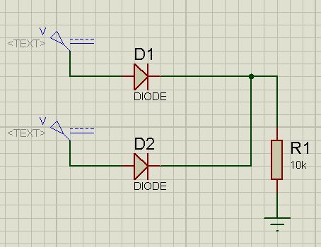
I saw this circuit in an electronics' book . In the first image , the voltage sources are the same for the 2 diodes, that's mean every diode will have 0.7 V and the resistor will have 4,3 V.

Voltage sources are equal

The problem was with the 2nd image, if I increase the first source voltage by 1 mV and decrease the second by 1 mV , the answer that the resistor will maintain its voltage to 4.3 V but what will change is the diode voltage :

Vd1 = 5.001 - 4.3 = 0.701;

Vd2 = 4.999 - 4.3 = 0.699;

difference between voltage sources

Can anyone tell me what will happen in the 2nd circuit, more explanations by a circuit analysis or any method to understand.

\$\endgroup\$
2
  • \$\begingroup\$ Are these theoretical perfect diodes, or real-world ones? The result will be different. But either way, I would expect the voltage across the resistor to change - to either exactly or approximately 4.301V. \$\endgroup\$
    – Simon B
    Commented Jun 7, 2017 at 9:32
  • \$\begingroup\$ No it's not possible , because with the first circulating current , it's 4.301, with the other it's 4.299 , and the value should be unique. \$\endgroup\$
    – Zara Zara
    Commented Jun 7, 2017 at 9:43

4 Answers 4

1
\$\begingroup\$

The circuit forms a simple form of an OR gate, so the lower voltage won't contribute to the current through R1 at all, thus can be completely ignored. The forward voltage is (aat least almost) constant, so the voltage over R1 will rise by dV.

\$\endgroup\$
1
  • \$\begingroup\$ sorry, no it's not , because we talk about a real diode which has an internal resistance and drops more or less than 0.7 V What you said is true if we have a difference of voltage between in range of 1 V the first and 2nd source. \$\endgroup\$
    – Zara Zara
    Commented Jun 7, 2017 at 11:08
1
\$\begingroup\$

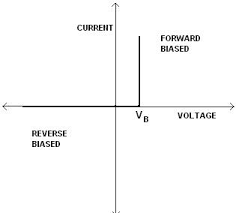
Assuming they are ideal diodes with a Vd of 0.7:

D1 will be forward biased so Vr1 is 4.301V

D2 will not be forward biased, so no current will flow since V-dV - 4.301 = 0,698; which is not enough to forward bias your ideal diode.

Vb in pictur is Vd in my comment

If the diodes where real, Vd would not be exactly 0.7 and the I-V relation would not be a vertical straight line, it would be a non-linear funcion with a slope affected by temperature and other factors. Wikipedia article "Shockley diode equation" covers it. Also noise in the power supplies should be taken into account. Summarizing, a lot more to take care of.

\$\endgroup\$
2
  • \$\begingroup\$ and in the case of read diodes ( diode + internal resistance), the 2 diodes will be on ? \$\endgroup\$
    – Zara Zara
    Commented Jun 7, 2017 at 11:04
  • \$\begingroup\$ I updated my answer. If it suits you accept it =) \$\endgroup\$ Commented Jun 7, 2017 at 11:16
0
\$\begingroup\$

let's take some assumptions :

Vs1 = V + dV

Vs2 = V - dV

Diode : diode + internal resistor = Rb (real diode)

current circulating in the first diode = i1

current circulating in the 2nd diode = i2

total current in resistance = i

i1 + i2 = i

i1 = (Vs1 - Vd - Vr)/Rb i2 = (Vs2 - Vd - Vr)/Rb i = Vr/R

(Vs1 - Vd - Vr)/Rb + (Vs2 - Vd - Vr)/Rb = Vr/R .

(V+dV - Vd + V-dV - Vd)/Rb = Vr(2/Rd + 1/R)

with Rb = 1 ohm .

2V - 2Vd = Vr(2R + Rb)/R

Rb <<< R

Vr = V - Vd = 5-0.7 = 4.3 V

Vd1 = 5.001 - 4.3 = 0.701 V (+ 1 mV across Rb1)

Vd2 = 4.999 - 4.3 = 0.699 V (- 1 mV across Rb2)

\$\endgroup\$
0
\$\begingroup\$

Your question is made unclear by your comments to the other answers.

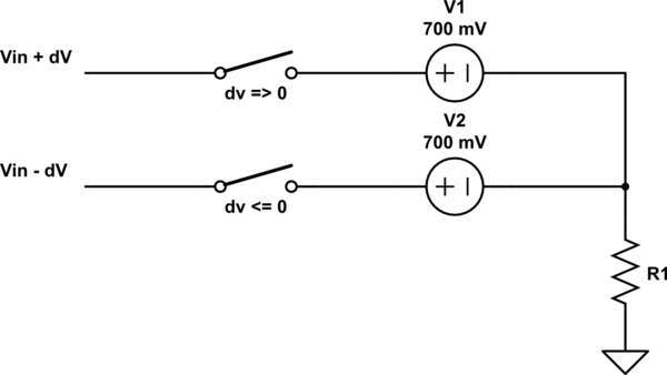
If this is a theoretical question using ideal diodes then in the second case only the diode with the larger voltage attached will be conducting and the voltage across the resistor will have that voltage minus 0.7V across it.

For this circuit it can be modeled as follows with two switches.

schematic

simulate this circuit – Schematic created using CircuitLab

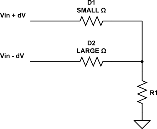
If they are in fact real diodes it is more complicated and the circuit becomes the following.

schematic

simulate this circuit

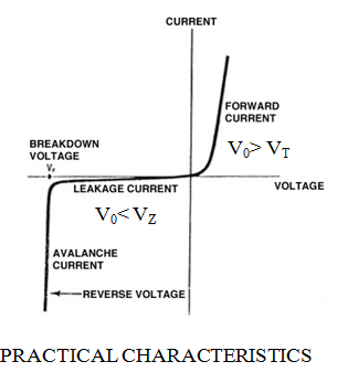
\$LARGE \Omega\$ becomes EXPONENTIALLY greater than \$SMALL \Omega\$ as \$dV\$ increases. As dictated by the devices non-linear conduction curve. NOTE: The slope of that curve is the devices conductance. i.e. \$1/R\$

enter image description here

Ultimately, if \$dV\$ is too large D2 will enter the zener region and avalanche breakdown will occur and it will again become low resistance.

\$\endgroup\$

Your Answer

By clicking “Post Your Answer”, you agree to our terms of service and acknowledge you have read our privacy policy.

Not the answer you're looking for? Browse other questions tagged or ask your own question.