0
\$\begingroup\$

For a highly-sensitive electrometer one needs not only high resistance but also a really small capacitance to achieve certain AC behavior e.g. stability of the opamp.

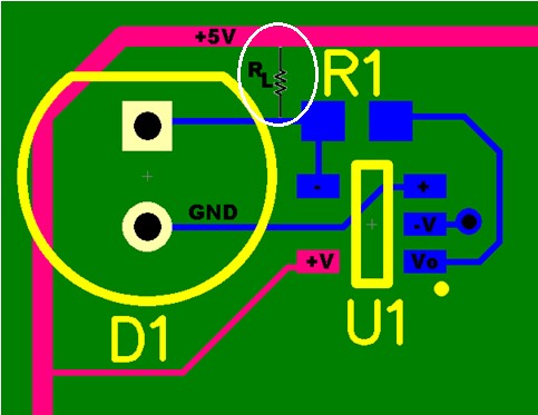
The figure below shows a typical example of a electrometer circuit with an opamp and can be extracted from this Analog Devices application note.

Layout of a electrometer.

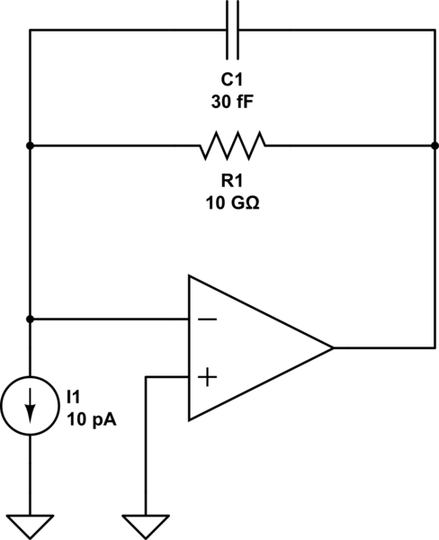
This is equal to the following circuit.
schematic

simulate this circuit – Schematic created using CircuitLab

The values given in the schematics plus the noise budget calculations I did, result in a output range (worst-case, \$T_A = 25°C\$) from \$320\, µ V\$ (noise floor) up to \$ 3.3 \, V\$ when a dual power supply (\$V_+=3.3 \, V\$ and \$V_-=-3.3 \, V\$) is used. According to simulation a \$3 dB\$ bandwidth of \$ 530.52 \, Hz\$ works well for a pulsing of the input signal with \$ 200 \, Hz\$. The idea is suppressing noise below this frequency as you mix your signal up from \$0 \, Hz\$ to a higher \$f_{IF}\$. The bandwidth of the system is mainly determined (or from a ideal POV only determined) by the feedback capacitor and can be calculated with

$$f_{3dB} = \frac{1}{R_f C_f 2 \pi}$$

So the capacitance needed is in the femtofarad range (\$30 \,fF\$). Now my question is if you have a feedback path (cf. picture), where you want to avoid coupling impedances (to somewhere outside of this low-current path) of any kind (you use all kind of fancy guarding techniques e.g. via fencing) would you say it is legitimate to use an embedded, self-made pcb cap? You know like basically two plates on TOP and BOTTOM.

I mean the calculations say, that for \$30 \, fF\$ you need two plates with an area of approx \$1.153 \, mm^2\$ when you use FR4 (\$\epsilon_r = 4.7\$) and a PCB with \$1.6 \, mm\$ thickness.

So you have

$$ C = \frac{\epsilon A}{d} $$

which can be rewritten as

$$ A = \frac{C d}{\epsilon} $$

If I got it correctly you can just draw two squares on the PCB on both sides, each of them has the following dimensions $$\sqrt{A} \cdot \sqrt{A}.$$

Conclusion: Can I use an embedded capacitance when working in the femtoampere (YES \$10^{-15}\$ A) range or am I missing out on something here? It is quite hard to get such small capacitances, which is the reason why a embedded capacitor shall be used.

\$\endgroup\$
2
  • 2
    \$\begingroup\$ I'm confused. You seem to mean "capacitance", not "capacity". But, you describe this "capacity" in Amps (current), not Farads (capacitance). Please edit your question to make it more clear! Thanks. \$\endgroup\$
    – bitsmack
    Commented Jun 28, 2017 at 17:14
  • \$\begingroup\$ Sorry. I corrected my mistakes. \$\endgroup\$
    – m3x1m0m
    Commented Jun 29, 2017 at 8:25

1 Answer 1

1
\$\begingroup\$

If you define your sensor as a Charge Meter with a sensor of 100 fF =\${10^{-13}}~~\$ [F] and a constant current of \$10^{-15} [A]~~\$ then

\$\frac{dV}{dt} = \frac{Ic}{C} = \frac{10^{-15}[A]}{10^{-13}[F]}={}{10^{-2}}{}[\frac{V}{s}] = t_R~~=\frac{0.35}{f_{-3dB}}\$ from 10% to 90% [V]

thus \$ f_{-3dB} = \frac{0.35}{10^{-2}}~=35 ~ \$ [Hz]

This \$ f_{-3dB}~~\$may be too high for your expectations.

Potential Solutions:

  • reduce stray C by using active guarding around tracks with same CM voltage buffered adjacent to signal tracks such that ΔV=0 thus ΔIc=0 between guard tracks and even less to stray conductors.
  • use chopper stabilized methods in datasheet.
  • use lower input bias current Op Amps.
  • reduce stray leakage R by using air tracks to reduce surface dust creepage R as explained in datasheet
  • Compute track PCB capacitance which is 4x air to reduce conductor capacitance to sensors using wider separation and air tracks perhaps with AWG 30~40 magnet wire.
  • use gold leaf sensors and measure displacement like Coulomb did which had a long decay time [s]
  • use circuits employed for ESD meters to measure discharge or charge with S&H with suitable protection. They often use a charge amplifier (TIA) commonly used for large piezo accelerometers to measure vibration charges to convert to voltage but maybe also BW limited.

Comments?

\$\endgroup\$
7
  • \$\begingroup\$ Thank you for your answer. I had another approach calculating the \$ f_{3dB}\$. $$f_{3dB} = \frac{1}{R_f C_f 2 \pi}$$ You can get this equation by using \$ P = U \cdot I^*\$. So this would result in approx. 160 Hz. It is nothing more than a parallel resonant circuit consisting of R and C. I can not just put C to 0 as I have a pole. So you can see in the LTSpice ac analysis, that it is escalating at some point. That is why I need a capacitance. A really small one. And my question is: Can I do this by putting an embedded capacitance in the feedback loop or will this have negative side eff.? \$\endgroup\$
    – m3x1m0m
    Commented Jun 29, 2017 at 8:40
  • \$\begingroup\$ To improve s21 gain + phase response we need you to give a spec and schema model on your requirements. Then it will be obvious what to do with phase margin using the correct source capacitance and lead-lag compensation circuit. \$\endgroup\$
    – D.A.S.
    Commented Jun 29, 2017 at 13:54
  • \$\begingroup\$ I edited the original post. \$\endgroup\$
    – m3x1m0m
    Commented Jun 29, 2017 at 22:08
  • \$\begingroup\$ @m3x1m0m by specs I mean what are your requirements for Signal Input, Output, SNR, Signal BW, Noise BW, dynamic range, and accuracy requirements for calibration, limitations on sensor size, etc. \$\endgroup\$
    – D.A.S.
    Commented Jun 30, 2017 at 5:34
  • \$\begingroup\$ I hope I collected all the information needed to design such a system properly now. It is not a communication system so I do not really have a SNR. But I guess, that is OK? Basically everything above the noise floor (\$320 \, µ V\$ worst-case at the output) is visible. \$\endgroup\$
    – m3x1m0m
    Commented Jun 30, 2017 at 8:41

Your Answer

By clicking “Post Your Answer”, you agree to our terms of service and acknowledge you have read our privacy policy.

Not the answer you're looking for? Browse other questions tagged or ask your own question.