Not clear from your question and from documentation - you created device in library editor, then to change this device's pad properties you need to go to library editor, do it there and then update device in the circuit/board; you will not be able to make change to pad which is a part of the device in board editor.
When in library editor, you can change diameter of the pad using info tool in the GUI.
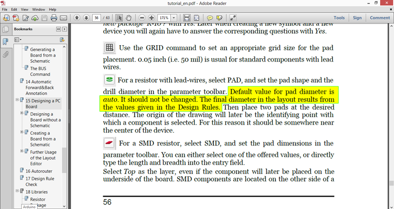
The related design rules are located in the DRC -> Restring tab, where you can set pads' minimum and maximum diameter, and percentage of their drill diameter.
The recommendation It should not be changed prevents you making a lot of custom pads and vias which do not comply with settings on that DRC tab, and thus getting a lot of errors which you will have to manually correct in the library editor, or will need to change settings in DRC rules. For advanced EAGLE user it would be ok, but if you are a beginner, you will get lost and hate the tool at the end.
Let's look at what "pad diameter" is. It is a space to put solder into to fixate the component's pin. Default design rules are defined the way so that you would be more or less easily solder the pins, contact would be good and part would be fixed on the board well.
Why you may need to change the pad diameter from auto (in other words - from default rules' settings)?
- To make its solderable area bigger (most probably not smaller!). I used to do it, it is normal, but as I said if there will be something wrong in the layout at the board level you will get an error.
- To open some space on the solder mask - do not forget that pad is an area uncovered by the mask.
How to avoid making big "non-standard" pads? Just cover pads with polygon with the same signal name, for example, ground pad may be size of auto, but when you cover it with polygon they merge forming big conductive area - this way you have only small pad's copper area exposed for soldering, and remaining space covered by the solder mask.

