4
\$\begingroup\$

How can a MOSFET cascode be explained (not calculated) intuitively? https://commons.wikimedia.org/wiki/File:MOSFET_Cascode.png#/media/File:MOSFET_Cascode.png
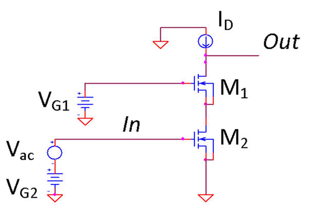
Especiall I would like to know why it's output resistance is high and why the drain voltage of the lower MOSFET M2 is stabilized, i.e. changes very little when the ouput voltage (Out) is changed.

Would this be a correct explanation?

  1. VG2 voltage determines the current going into the drain of M2. This current has to be the same for M1.
  2. Gate-source voltage of M1 (= VG1 - drain voltage of M2) is adjusted so that the drain current of M1 is equal to the drain current of M2.
  3. If output voltage (Out) is changed, the drain current of M1 would change due to the channel-length modulation of M1. But as the current of M1 has to be the same as the current of M2, the drain voltage of M2 (and thus the gate-source-voltage of M2) changes so that the currents are equal again. And this change is very small because the I_drain(U_drain_source) curve of a MOSFET is relatively flat and the I_drain(U_Gate_Source)-curve of a MOSFET is very steep. Therefore a big change of the Out voltage causes a very small change of the drain voltage of M2 (voltage is stabalized here). Therefore the current changes not much and the output resistance of the cascode is very high.
\$\endgroup\$
4
  • \$\begingroup\$ If you are asking questions about the output impedance being high then you are not beginning at the right point. Do you understand why the output impedance of a common emitter (or common source) amplifier is high? \$\endgroup\$
    – Andy aka
    Commented Jul 24, 2017 at 16:27
  • \$\begingroup\$ Yes, the output impedance of a common source amplifier is high because the MOSFET ID-VDS characteristics show in saturation nearly a horizontal line. Right? So if the upper explanation is not accurate, is it possible at all to explain it in a descriptive way, let's say based on the MOSFET characteristics? \$\endgroup\$
    – Jo123
    Commented Jul 24, 2017 at 17:38
  • 3
    \$\begingroup\$ I don't like your explanation but I like mine.... M1 is a source follower so it sets a near constant voltage on M2 drain. This means M2 doesn't suffer from miller capacitance effects. Current through M2 drain is transferred to a voltage at M1 drain because of the high compliance of the current source (normally a resistor). \$\endgroup\$
    – Andy aka
    Commented Jul 24, 2017 at 17:50
  • \$\begingroup\$ Ok. Thanks!! I've to look up what a source follower is in order to understand your response. \$\endgroup\$
    – Jo123
    Commented Jul 24, 2017 at 18:21

1 Answer 1

2
\$\begingroup\$

To answer this question, I will try to build the above circuit which you have step by step and explain intuitively at each step. I will take N-MOSFET for simplicity.

If we take a simple transistor (operating in saturation), its a current source. Therefore, in ideal conditions at saturation, the drain current should not depend on Uds but due to channel length modulation, there exists a small dependence of the drain current on Uds. Basically the above cascode connection (in question) tries to minimize the voltage fluctuation at the M2 Drain terminal. This is called "shielding effect" and is responsible for high output resistance of the cascode structure.

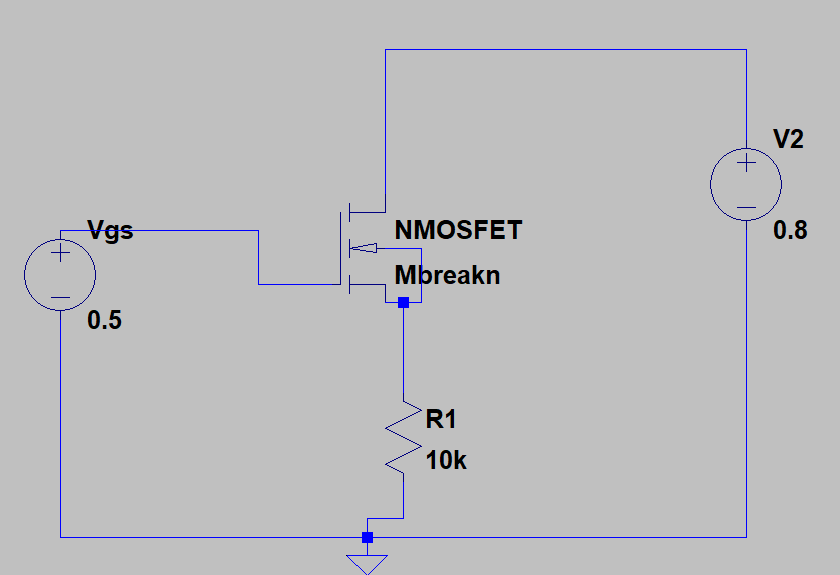
Now, if we consider a simple Widlar Current Source as shown below,

enter image description here

This circuit has normally has a high output impedance due to the feedback connection. Understanding this circuit intuitively will help in understanding of cascodes.

Operation: In this circuit, if we cause a voltage jump at the Drain terminal, the voltage jump seen at the Resistance (Source terminal) is very low.

This is because:

  1. As we increase Vout, Id increases.
  2. The more current causes more voltage drop across R.
  3. Hence Source potential increases and Ugs decreases.
  4. Since Ugs has decreased, hence Id decreases too.
  5. So, current is reduced again causing the same voltage drop across R which was present before. (more or less same)

The output resistance is also increased as we saw from the above explanation. Since its a feedback connection (Series-Series), output resistance can also be computed easily and increased dramatically by a factor of intrinsic gain (gmRds).

The above structure can also be seen as a Common-Gate Transistor because Gate is common between Input and Output.

Now in the cascode structure in the question, its a Common-Source and Common-Gate Cascode. The output resistance seen at the drain terminal of M2 is Rds of the transistor M2. So, applying the same analogy that we discussed in the widlar current source, the fluctuation at the output terminal is less at the drain terminal of M2 due to the transistor M1. This is called as Shielding property and hence high output resistance. Hope this helps.

\$\endgroup\$

Your Answer

By clicking “Post Your Answer”, you agree to our terms of service and acknowledge you have read our privacy policy.

Not the answer you're looking for? Browse other questions tagged or ask your own question.