2
\$\begingroup\$

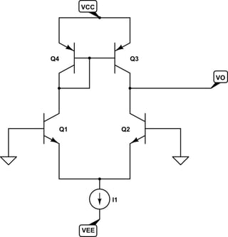
I want to compute the value of VO.

schematic

simulate this circuit – Schematic created using CircuitLab

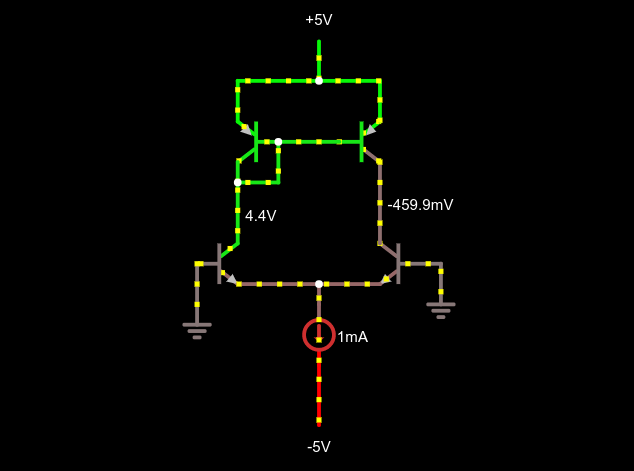
I would have guessed that VO = VCC - VEB. Asuming VCC = 5V and VEB = 0.6 V, that would render VO = 4.4 V, as in the left branch of the circuit.

But doing the simulation I found that VO is actually much lower: VO = -459.9 mV

enter image description here

So, how should I do to compute VO properly?

\$\endgroup\$
1
  • 1
    \$\begingroup\$ Calculating Vo in a circuit like this is a fool's errand. This is a differential amplifier. The voltage you will see if you build the circuit depends on subtle differences between Q1 and Q2 and is unpredictable. It is similar to the output offset voltage of an op-amp. You don't know how big it will be or in which direction. It is a useful circuit, but the output is not defined when the differential input measured across the bases of Q1 and Q2 is near zero. \$\endgroup\$
    – user57037
    Commented Jul 29, 2017 at 19:00

4 Answers 4

2
\$\begingroup\$

The DC output voltage of a differential pair isn't a particularly useful figure. As with any input offset voltage from mismatch the output will rail one way or the other.

The simple answer is that all your PNPs are matched and your NPNs are matched.

So, in the left-hand branch you have an extra \$2I_b\$ from your current mirror.

The left NPN has a \$V_{be}\$ which is based on this extra \$2I_b\$. The right NPN has the same Vbe but see's 2Ib less collector current than the other branch. So the right NPN saturates trying to pull the same current as the left NPN.

\$\endgroup\$
0
\$\begingroup\$

You're correct that, in theory, those voltages are equal. In real life offsets between the two devices will result in that not being true. However, simple simulations such as the one you're using don't model offsets. So one would expect the voltages to indeed be equal.

What your software does, however, model is finite beta of the transistors.

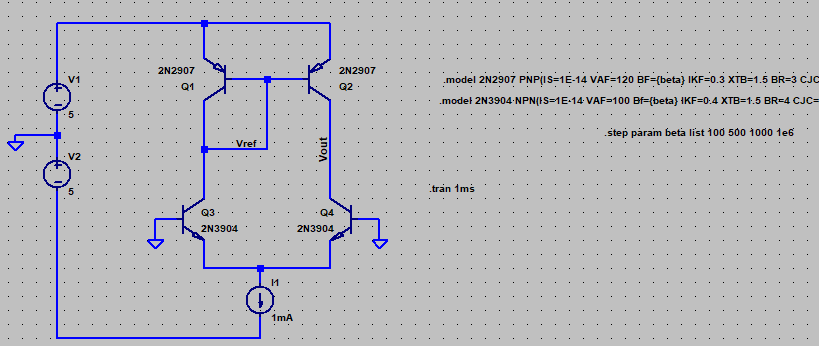
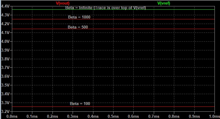
Here is a simulation I did, where I swept the Beta of each device from 100 to 1e6 ("infinite").

You can see how Vout approaches Vref as beta -> infinity.

Diff. Pair Schematic

Waveform

You can get an intuitive "feel" for the fact that finite beta affects this circuit by noting that Q3 pulls two base currents in addition to the current "programmed" to the collector of Q1.

\$\endgroup\$
0
\$\begingroup\$

You can calculate Vo by making the unrealistic hypothesis that all transistors are perfectly identical. This will not be the case using real transistors though, so this calculation is useless.

Q1 and Q2 form a long tail pair differential amplifier. They take as input the voltage difference between their bases, and output a difference in collector currents. It is important to notice that the output is a current, not a voltage.

Here, both bases are at the same potential. Using the unrealistic hypothesis that both transistors are identical, their collector currents are thus equal, and their value is I1/2 minus the base current, which we will neglect.

Now, Q3 and Q4 form a current mirror. Q1's collector current is mirrored and output by Q3. Q3's collector current is thus I1/2 also.

Q3 and Q1's collector currents thus cancel perfectly and... we forgot Q3's base current. We can't neglect it this time.

Thus, after the I1/2 parts in Q1 and Q3 collector currents cancel, the current which attempts to flow into node "Vo" is the base current of Q3, which is negative.

With I1=1mA and Q3 having a hFe of 200, this current is 1mA/2/200 = 2.5µA

However, we neglected Early effect (and self heating) in all transistors, which we really shouldn't be doing. So this value will be wrong.

Anyway. You want voltage. This means we have to compute the impedance at node Vo, to convert current into voltage. Bad news is this impedance is difficult to compute, since two collectors are facing each other. It will depend on individual transistor characteristics, ie their parapeter ro (due to Early effect).

What you are seeing is that the collector impedance of your transistors is high enough so that output voltage clips against one of the transistors.

This circuit should be used with a low input impedance stage after it, which takes a current as an input, and imposes a voltage to point Vo.
\$\endgroup\$
0
\$\begingroup\$

I will try to explain how the circuit works intuitively. Q3 and Q4 form a current mirror. This means that their collector currents will be very nearly equal over a wide range of collector voltages. Or you could say that the current will try to be equal, unless it is just not possible.

Next thing to notice is that the total collector current is fixed because of the current source. Let's call that Itot. So Icq1 = Icq2 = Itot/2.

Now let's look at Q1 and Q2. These are the input pair of this differenatial amplifier. Basically, if the base of Q2 is higher than the base of Q1, then Q2 will try to conduct more current than Q1. But the current mirror will try to keep the collector currents equal. The net result of this is that when Q2's base goes high, Q2's collector goes low, and Q1's collector goes high. The reverse is also true.

Without any feedback or anything, this acts like a comparator, shooting from rail-to-rail depending on which base, Q1 or Q2 has a higher voltage. If you add gain stages and some feedback, you will have some kind of rudimentary op-amp.

Hope that helps.

\$\endgroup\$

Your Answer

By clicking “Post Your Answer”, you agree to our terms of service and acknowledge you have read our privacy policy.

Not the answer you're looking for? Browse other questions tagged or ask your own question.