0
\$\begingroup\$

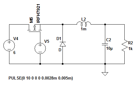
Here's a very basic buck converter circuit. The goal is to convert a 6V battery source into a fixed 3V output.

enter image description here

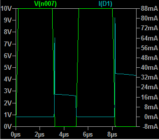
The efficiency of this converter is about 60%. That's not any good at all and I tried to see if I could come up with a much better model so that the efficiency could be improved by at least 30%. The problem with the above circuit is that when D1 is on it consumes a small amount of power.

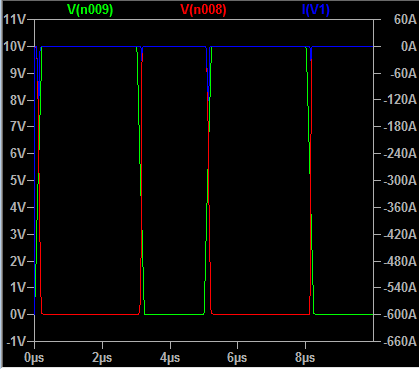
To remedy this I noticed that M5 and D1 work exactly 180 degrees out of phase, i.e. when one is on the other is off and vice versa. This can be seen in the following diagram:

enter image description here

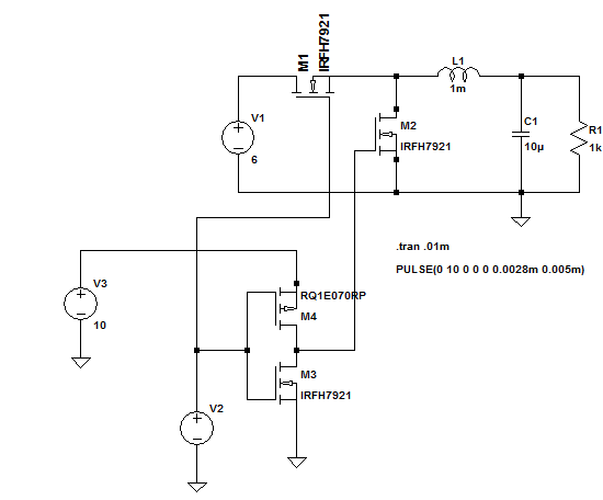
This gives me the idea of replacing D1 with an ideal switch element so that when it's on it doesn't waste much power and when it's off it acts like an open circuit. I thought of an NMOS as the replacement for the diode:

enter image description here

Though it should solve the problem of D1's consumption it actually doesn't much. I'm getting strange current readings out of input voltage source, and other MOSFETs. Here's a snapshot of the input voltage current, and gate voltages of M1 and M2.

enter image description here

I'm not sure what's wrong with the above circuit. I don't know if there need to be some delay between the turning on and off of M5 and D1 which I haven't considered in my model. Any help is appreciated.

\$\endgroup\$
4
  • \$\begingroup\$ Yes, there has to be a delay otherwise you have a short around the voltage source and both transistors. The diode doesn't have this problem because it can only conduct in one direction. \$\endgroup\$
    – Janka
    Commented Sep 3, 2017 at 19:56
  • \$\begingroup\$ You need a diode after the output inductor. \$\endgroup\$
    – tuskiomi
    Commented Sep 3, 2017 at 19:58
  • 1
    \$\begingroup\$ @tuskiomi: No, that shouldn't be necessary. \$\endgroup\$
    – Dave Tweed
    Commented Sep 3, 2017 at 20:01
  • \$\begingroup\$ This is called synchronous rectification, and is a good way to boost efficiency at larger load currents. However, as @Janka mentions you need a delay between turn-off and turn-on to avoid shoot through, which will kill your efficiency or even your FETs. You can put a Schottky diode across the low side FET to reduce the drop during the time when both switches are off. \$\endgroup\$
    – John D
    Commented Sep 3, 2017 at 20:05

1 Answer 1

2
\$\begingroup\$

Why are you using an N-channel MOSFET as a high-side switch? That's where your efficiency is going — into excessive drop across the MOSFET.

The IRFH7921 is intended to be used as the synchronous rectifier (i.e., the low-side switch) in a synchronous point-of-load converter. You need a P-channel MOSFET for the high-side switch.

\$\endgroup\$
1
  • \$\begingroup\$ Or you could use a bootstrap cap and high side driver to drive an N-MOS high side switch. An NMOS will be cheaper and smaller die size for the same RDSon. \$\endgroup\$
    – John D
    Commented Sep 3, 2017 at 21:02

Your Answer

By clicking “Post Your Answer”, you agree to our terms of service and acknowledge you have read our privacy policy.

Not the answer you're looking for? Browse other questions tagged or ask your own question.