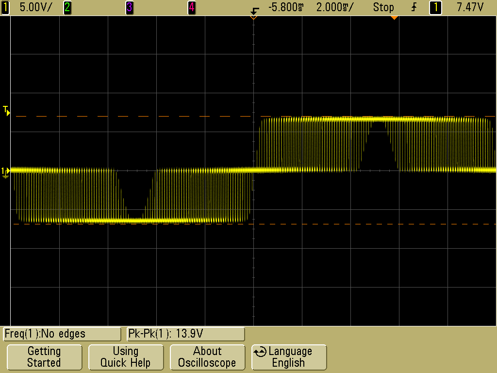
I have built an AC/DC pure sine wave inverter (SPWM). My inverter is a full H-Bridge NMOS (IRF630) setup and the gate is being driven by a 4N37 optocoupler. My input DC signal is 12VDC and this signal is also being used for my optocoupler to fire the gate of my high and low side mosfets. The output of my inverter is the following (Rl=100ohm) 
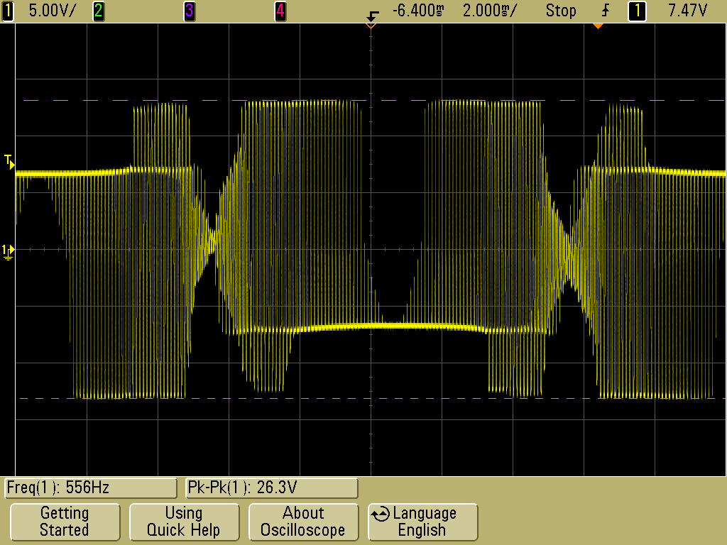
I have designed a low pass LC filter using L=68mH (Inductor 686C) and C=42uF to give me a cut-off frequency of approx. 94Hz. When I connect my filter to the output of my mosfets and connect a 100 ohm load I get the following output waveform.[![Figure 2: Inverter output of Filter][2]][2] I am assuming the the flat spot in my output AC waveform is due to the duty cycle imperfection approaching 100% duty cycle because of the switches not being ideal switches. Now when I connect my probe to check my input signal to my LC Filter expecting it to be similar to the of Figure 1. My oscilloscope now shows that the input signal is now greatly distorted. [![Figure 4: Close up of transients][4]][4] It seems to show that the inverter output response has become underdamped when connected to the LC filter. Is this happening due to impedance mismatch between my load and my source? If so how does impedance mismatch lead to an underdamped response? What is a possible approach to creating a matching circuit if this is the case? If not the case, what else is causing this distortion to my input signal? Parasitics of Inductor? Poor Inductor material Selection?? Also, When I disconnect my load the output waveforms seem to be approximately the same.
