0
\$\begingroup\$

I've been working on a project to build a microphone in DIY after finishing my audio engineering internship, but it seems like my knowledge in electronic isn't good enough to fully understand what i'm doing here.

The microphone is working great after the build, but the constructor gave no informations on the PCB schematic and what they are intended to do in the circuit. I would like to know what both PCB are doing in just few words, any tips would be very helpfull as it is quite hard to find precise informations on microphone PCBs, especially for a frenchie!
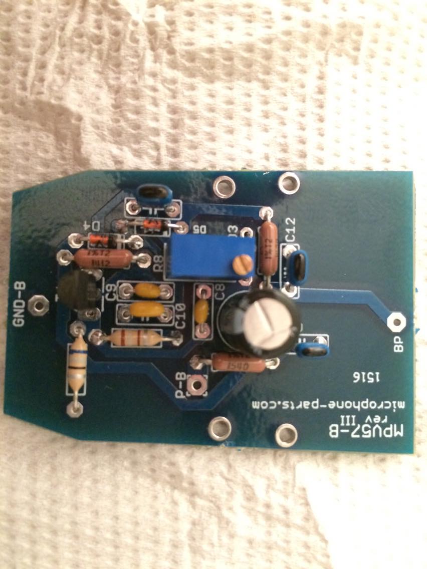
https://imgur.com/a/f6rNV PCB B

https://i.sstatic.net/Tf03N.jpg PCB A

I have been told from an electronic store guy that they are intended to take the extremely small charge variation from the capsule and convert it to a voltage, but that is all the informations he gave me. I also believe this are originated from Schoeps circuit.

Any help would be great, i would really like to understand what's goind on in there!

Thanks,

Cheers

\$\endgroup\$
3
  • 2
    \$\begingroup\$ These are likely the things we, in engineering, call as "amplifiers". They take small charge variations in a microphone and convert them into voltage. What kind of "audio engineering" are you in? \$\endgroup\$ Commented Sep 12, 2017 at 22:23
  • 1
    \$\begingroup\$ I used to design B format mics (And the associated signal processors) for a living and would have been fired for coming up with this dogs dinner. \$\endgroup\$
    – Dan Mills
    Commented Sep 12, 2017 at 22:46
  • \$\begingroup\$ Thanks for the answers that means a lot! I used to be in a 3 year audio engineering school but we didn't study that much electronic there, so i'm kind of trying to catch up with what i missed. This is totally unecessary because i basically spend all my time on Protools, but it is always better to know more about what you are working with i guess! \$\endgroup\$
    – Ja Mertz
    Commented Sep 13, 2017 at 13:07

2 Answers 2

3
\$\begingroup\$

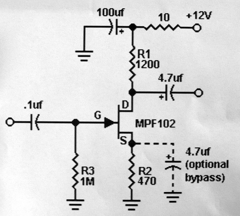
This circuit is basically a really simple JFET amplifiers with supply filter and a pot for adjustable attenuation, similar to this. enter image description here

The JFET is a voltage controlled voltage source which can offers a high impedance input like 1M and lowers the output impedance but is still considered high impedance as it is must a single transistor pre-amp with a voltage gain of less than 10 and an attenuator pot. That's a guestimate based on the very primitive description.

scam alert

From looking at the website, I don't have anything good to say about them and their price gouging and unprofessional content is alarming. What they offer is worth at best $10 in parts for a sale price of $168.02 is unethical IMHO.

If you did not get a schematic with the kit, I feel sorry for you and shame to anyone who advised you to get this DIY kit. They also have linear circuit DIY kits for $269 . (obvious scam)

e.g. they mention here a pre-biased NOS FET, which sounds amazing as this is a fake identification that does not exist, except on other sites that reference the same parts NOS FET meaning "New Old Stock".

The circuit will most likely contain a "JFET biased pre-amp" of dubious quality.

My only advice if you have one is to ensure when soldering the parts, that solder flows thru the plated thru holes incase they are bad. This only takes 3-5 seconds with a clean iron tip while applying solder. No more than 5 seconds.

Then avoid this site as it is a scam DIY kit site. Amazon and Ebay have much better completed boards for 10% of this cost.

P.s.

If you are really anxious to try simple DIY kits , consider something like this. http://talkingelectronics.com/projects/200TrCcts/200TrCcts.html#34 but keep in mind this is like 20~40 yr old technology... but at least it is only a kit of 15au$ from which you can make upto a dozen different simple circuits.

\$\endgroup\$
6
  • 1
    \$\begingroup\$ I guess this is called "business" in a market with good price elasticity... \$\endgroup\$ Commented Sep 12, 2017 at 22:32
  • 1
    \$\begingroup\$ A business with a gmail address? Srsly? \$\endgroup\$
    – Ian Bland
    Commented Sep 12, 2017 at 22:52
  • 1
    \$\begingroup\$ OMG. The price markup is surreal. \$\endgroup\$
    – bobflux
    Commented Sep 12, 2017 at 22:56
  • \$\begingroup\$ These guys seem to feed on a special layer of customers, same layer who buys Monster audio cables for their "deep, tight bass and smooth, natural midrange" response. \$\endgroup\$ Commented Sep 12, 2017 at 23:42
  • \$\begingroup\$ Well, they are currently the N°1 site on DIY microphone as far as popularity and such, so i wanted to try out their stuff. Their capsules are pretty good, even tho pretty simple compared to other stuff you can find. I would say the overall microphone quality is good, but definatly not what i expected for that price (roughly 400€ with a 90€ import tax from the US... that hurts). Already have a new business in mind to try out so it is all good! \$\endgroup\$
    – Ja Mertz
    Commented Sep 13, 2017 at 13:26
2
\$\begingroup\$

Not supplying a schematic with a kit is horribly poor IMHO, especially as PCB A is pretty clearly based on a CMC-6 impedance converter at least in part.

T3 is pretty clearly one of the impedance converters, but the presence of the omni/cardioid switch tells me that there should probably be another one hiding there somewhere, or maybe something clever/ugly is being done, difficult to tell.

T1 & T2 are the line drivers which also supply the DC supply to the rest of the circuit (Find a copy of the CMC 6 mic amp, it is all over the net), yours is similar in this area.

I Think PCB B is power doings, possibly an oscillator around that transistor and a voltage multiplier or something? Knowing what the instructions for that trimmer were and how the BP pad connects to the rest would help clarify things. I hope there is at least one 1G ohm or so resistor installed air wire style?

\$\endgroup\$
3
  • \$\begingroup\$ Well, the trimmer is a 2k Ohm potentiometer (R8, blue trimmer on PCB B), turning his screw will lower the impedance of R8 and raise the capsule polarization voltage. This adjustements takes place at the end of the build, when checking and adjusting the voltage going into the capsule (using a multimeter, ideal voltage is said to be 60V). The BP pad is connected to the backplate wire of the capsule, and both PCB are connected by the GND pad. The frond diaphragm of the capsule is soldered with the 3-way joint (3 way beetwen the JFET J305, the 1G ohm resistor and the switch) on PCB A. \$\endgroup\$
    – Ja Mertz
    Commented Sep 13, 2017 at 13:49
  • \$\begingroup\$ Ok, so PCB B is the polarisation supply doings, pretty much as I thought. With only two connections from the capsule I am puzzled by the operation of the omni/cardioid switching? \$\endgroup\$
    – Dan Mills
    Commented Sep 13, 2017 at 14:00
  • \$\begingroup\$ This was indeed one of the "problem" i had with the build. The switch configuration enables you a Cardioid and Omni pattern with the rear diaphragm also soldered to the 3 way joint. It also enable you to have a Cardioid and -10dB PAD without connecting the rear diaphragm of the capsule, but the Omni pattern cannot be used anymore so i had to choose. In my case , a -10dB PAD seems more usefull so i choose not to use the rear diaphragm, wich makes only two connections from the capsule. That was pretty disapointing to be honest,on top of that there is no external switch on the microphone case. \$\endgroup\$
    – Ja Mertz
    Commented Sep 13, 2017 at 15:50

Not the answer you're looking for? Browse other questions tagged or ask your own question.