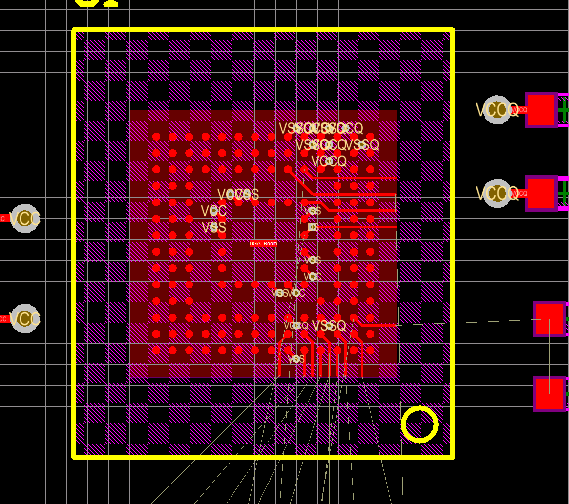
I have placed my first BGA on a PCB. I have followed the instructions from this video:
How to fanout a BGA - Altium Designer 16.1 - Joao Beck
The overall footprint of the BGA is much larger than the pad area and so my room does not totally encompass the entire component footprint. Regardless, my BGA fanned out nicely.
However, now when I run my DRC, I get the following error:
Room Definition: Between BGA Component on Top Layer And BGA_Room (Bounding Region) (All)
Note: I also removed the default room from the schematic using this method.
What does this error mean? How do I resolve it?

