1
\$\begingroup\$

I have a few questions regarding using the DMA of the stm32f7 board (nucleo F722ZE ).

1) So to get started I'll explain what I'm doing:

I need to read data from 2 GPIO pins (ADC) and will have a clock signal fed to the stm32f7 from the device supplying the data. I plan on letting the clock signal trigger an interrupt timer and whenever the timer is triggered I want the DMA to do a memory to peripheral transfer. The memory will be 2 bits on the GPIO port with the peripheral being a SPI line coupled to a SD card.

2) Accessing the data:

I referred to the arm cortex 7 manual and found the following:

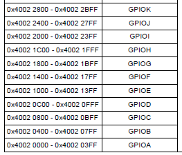
The GPIOC port is mapped to 0x40020800 - 0x40020BFF and the input data registers are set at an offset of 0x14.

So I take the memory mapped base register (0x40020800 and add 0x14 to it) Therefore the source address I supply to the DMA will be 0x40020814?

3) Having the DMA shift out this data.

This might be the larger problem. Once I have the data at the GPIO pins, I'll essentially be receiving it bit for bit and the data is actually 24 bits long, per pin. So in total each gpio pin will receive 24 bit packs of data. Although when the external signal triggers the timer, I'll only have one bit at each of the GPIO's.

Is there any way that the DMA can selectively pull out the data bit by bit, till it has all 24 bits and then send it over the SPI. Using some sort of buffer and burst transfer? Otherwise it seems the DMA can do a minimum of a byte transfer, which will require me to send massive amounts of garbage bits for every bit I transfer.

Finally: To summarize, I'm uncertain about the location of the GPIO data, is the address I put down correct and I'm completely unsure of how to go about having the DMA transfer this data??

Any help will be appreciated!

\$\endgroup\$

3 Answers 3

1
\$\begingroup\$
  1. GPIO is not the ADC. I do not understand what you mean. If is an external ADC it probably transfers it using standard interfaces like I2C or SPI. If you want to read the analog data you need to use then the internal ADC
  2. You have everything defined in the CMSIS headers. You do not need to think about the physical addresses. you will access the GPIO registers whis way : GPIOA -> MODER for example. There are all bits definitions as well in the human readable form.
  3. DMA does not transfer bits only bytes, halfwords or words. But you need to consider more smart way of reading them than toye inital idea. As you did not write what is the device connected I cant help you more.
  4. My advise - start from something easier - learn how to use CMSIS and the peripherals in your micro. I am 100% sure that you can use one of the standard ones: I2C, SPI or U(S)ART for it without any bitreading from the GPIO
\$\endgroup\$
0
\$\begingroup\$

1) This sounds like SPI. Do we have an XY-Problem?

2) You'd need the GPIO port input data register (GPIOx_IDR) (x = A..K), which is at offset 0x10 from base GPIO peripheral. Base address of each peripheral are found in the stm32f7 header or Table 1 of reference manual. (RM0385: Table 1) Table 1. STM32F75xxx and STM32F74xxx register boundary addresses (continued)
You can access GPIO registers in in word, half word or byte mode. (RM0385: 6.4)
Note: you can't access all peripherals in all widths.

3) It isn't the most efficient way with the DMA, bitrate would be low (kHz), but it can be done.

  1. Have the DMA read the byte on trigger to memory buffer (circular). (or words if the gpio's are far apart)
  2. At DMA Complete/Half IRQ, assemble the word from the DMA buffer. It would be nice if you had bitbanding, but the Cortex M7 lacks this.
  3. Process the word. Preferably in another function to keep the bitbanging layer separate from data processing.

Outputting bits with DMA works the same, except then you must use the GPIO port bit set/reset register (GPIOx_BSRR) (x = A..K) to not change irrelevant IO.

\$\endgroup\$
2
  • \$\begingroup\$ The problem is that there are 2 bits incoming at once, a single SPI controller can not handle that. \$\endgroup\$ Commented Oct 7, 2017 at 13:35
  • \$\begingroup\$ @berendi You have two synchronized ADC's, externally clocked, feeding data? If so, why not use two spi's, or maybe DFSDM? \$\endgroup\$
    – Jeroen3
    Commented Oct 7, 2017 at 18:57
0
\$\begingroup\$

a SPI line coupled to a SD card

The STM32F722ZE has dedicated SDMMC interfaces that are significantly faster than SPI, especially if you connect all 4 data pins.

So I take the memory mapped base register (0x40020800 and add 0x14 to it) Therefore the source address I supply to the DMA will be 0x40020814?

That would be fine if you got the address right (IDR is at offset 0x10), but it would be even better to use the definitions from the standard headers

DMAx->SyPAR = (uint32_t)&(GPIOC->IDR);

and then it'd be obvious to everyone looking at your code what this piece of code is about. In addition, it helps avoiding mistakes in the address calculation.

Is there any way that the DMA can selectively pull out the data bit by bit, till it has all 24 bits and then send it over the SPI.

Connect each data line to a different SPI controller (there are 5 of them), connect the clock line to both. Let them each fill up a 256 byte buffer (with DMA), adjacent to each other, to keep the SD controller happy with a block size of 512 bytes (2*2048 byte buffers may be even better). When the buffers are full, write the whole block to the card, while the SPI DMA channels can automatically switch to secondary buffers at a different address. You might want to use more than 2 alternating buffers to allow for filesystem updates, if you are using any (FATFS can be painfully slow updating the FAT table). I assume you can reassemble the bits later, when actually processing the data.

\$\endgroup\$

Your Answer

By clicking “Post Your Answer”, you agree to our terms of service and acknowledge you have read our privacy policy.

Not the answer you're looking for? Browse other questions tagged or ask your own question.