0
\$\begingroup\$

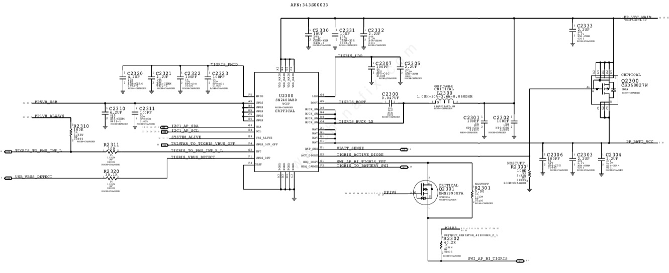
This is a charging ic/circuit from an iPhone and there aren’t any datasheets available for it.

I have a few questions:

  1. What would the purpose of the series capacitor c2300 on the switching side be for?
  2. What are PMID capacitors for?
  3. Why would q2301 be used if it looks to always be on when 1.8v is at the gate which is basically all the time when there’s power to the phone

Sorry if the picture isn’t clear it’s a screenshot from my phone

enter image description here

\$\endgroup\$
1
  • \$\begingroup\$ Lol sorry the app crashed on me. It’s loaded now \$\endgroup\$
    – user140123
    Commented Oct 18, 2017 at 11:46

2 Answers 2

0
\$\begingroup\$

This is a charging ic/circuit from an iPhone and there aren’t any datasheets available for it.

Of course not, Apple likes to keep everything secret as if we could not figure things out by reverse engineering if we wanted to.

c2300:

Looks like a boot-strap capacitor since it says something_BOOT on the left connection. Also the right is connected to the inductor and on-chip switch (note the 4 pins in parallel to carry a large current).

This is used to generate a voltage higher than the input voltage so that the gates of an NMOS can be pulled above the input voltage so that the NMOS can be fully on. One or more of such NMOS might be used as switches in side IC U2300.

PMID capacitors:

These might be supply decoupling capacitors for the bootstrap voltage made by c2300.

Or (less likely) decoupling of some other internal supply of IC U2300.

q2301:

I disagree that the gate of q2301 is always 1.8 V. Note that there is a net PP1V8_ALWAYS (which would always be 1.8 V) on the left but that gate is connected to PP1V8 suggesting that PP1V8 can some times be off.

\$\endgroup\$
9
  • \$\begingroup\$ Thank you. About c2300 being a bootstrap. Am I understanding right in that it’s used to boost the input voltage 5v to a higher voltage so that higher voltage can be bucked down to vcc ~4.2v? \$\endgroup\$
    – user140123
    Commented Oct 18, 2017 at 12:13
  • \$\begingroup\$ Yes, somehow in this design NMOS are used (instead of PMOS which would make things simpler, but anyway) and in order to switch on/off a 5V or 4.2 V line with an NMOS you need to pull the gate some volts above that 5 V. The bootstrap circuit creates the voltage needed for that. See: electronics.stackexchange.com/questions/111831/… for an explanation. \$\endgroup\$ Commented Oct 18, 2017 at 12:14
  • \$\begingroup\$ Is that bootstrap capacitor the clue that NMOS is used internally? Also in q2301 what do the internal diodes do? \$\endgroup\$
    – user140123
    Commented Oct 18, 2017 at 12:19
  • \$\begingroup\$ Yes, if they were using PMOS to switch the 5 V/4.2V then bootstrap is not needed. I know, I was in an SMPS design team couple of years ago. We used PMOS to avoid this bootstrap nonsense. NMOS can be smaller for same current though so using NMOS could make the chip smaller and cheaper. q2301: diode between gate-source is for (ESD) protection. The diode between drain and source is the drain-bulk diode, it is a parasitic diode that is always there, you cannot avoid it. All MOS transistors have a drain-bulk diode (and a source-bulk diode as well but here it is shorted). \$\endgroup\$ Commented Oct 18, 2017 at 12:24
  • \$\begingroup\$ Thanks again. One last thing, is there an advantage to using NMOS over PMOS? And if I measure voltage on the ic side of c2300 should I expect a voltage higher than 5v and if measured on the opposite end towards the inductor should it be at the buck voltage ~4.2v? Or would I measure the same voltages on both ends \$\endgroup\$
    – user140123
    Commented Oct 18, 2017 at 12:31
0
\$\begingroup\$

The C2300 is known as a bootstrap capacitor, it's used to drive switching mosfet gate above the VCC - Otherwise you'd have voltage dropout equal to the gate threshold voltage.

The other two components are not possible to know for sure without a datasheet and rest of the (legible) schematic. I'd hazard PMID are capacitors for the internal switching circuitry and Q2301 is probably a signal for "power good" condition after the voltages have stabilized. Might be tied to ENable somewhere.

\$\endgroup\$

Your Answer

By clicking “Post Your Answer”, you agree to our terms of service and acknowledge you have read our privacy policy.

Not the answer you're looking for? Browse other questions tagged or ask your own question.