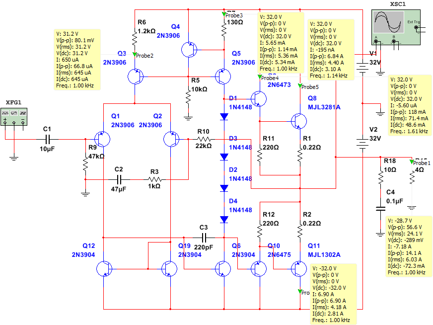
Can anyone draw (or write in text) the small-signal path from signal source XFG1 at input of Q1 base to amplifier load for positive and negative input signal swing?
-
1\$\begingroup\$ Pretty much every point in the circuit not fixed to +32V, 0V or -32V. \$\endgroup\$– FinbarrCommented Oct 24, 2017 at 16:12
-
\$\begingroup\$ Any amplifier is a "power supply" modulator. The input signal modulates the power supply current to create the input signal copy but with larger amplitude. Also, notice that in your amplifier the input stage and the VAS stage (Q6) work in class A. And the Output stage for low output power also work in class A. So it is not so easy to show how current flow. Also, what do you mean saying "small-signal path"? \$\endgroup\$– G36Commented Oct 24, 2017 at 16:38
-
\$\begingroup\$ Here you can find the example of an input current path for a CE amplifier. electronics.stackexchange.com/questions/310471/… Is this is what you have looking for? \$\endgroup\$– G36Commented Oct 24, 2017 at 16:39
-
\$\begingroup\$ I mean that the signal that goes from XFG1 with positive sinusoidal swing will close the Q1 and the base of Q6 will see the inverted signal that will open it. Then current will be inverted and two upper output bjts will be opening and the amplified signal will go into the load. But what is for negative input signal swing, how it will move? \$\endgroup\$– MaxMilCommented Oct 24, 2017 at 16:43
-
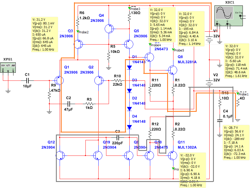
\$\begingroup\$ I also add how I see the DC voltage moving. Orange - Q1 is on, gray - Q2 is on. \$\endgroup\$– MaxMilCommented Oct 24, 2017 at 16:46
1 Answer
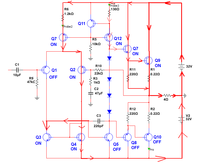
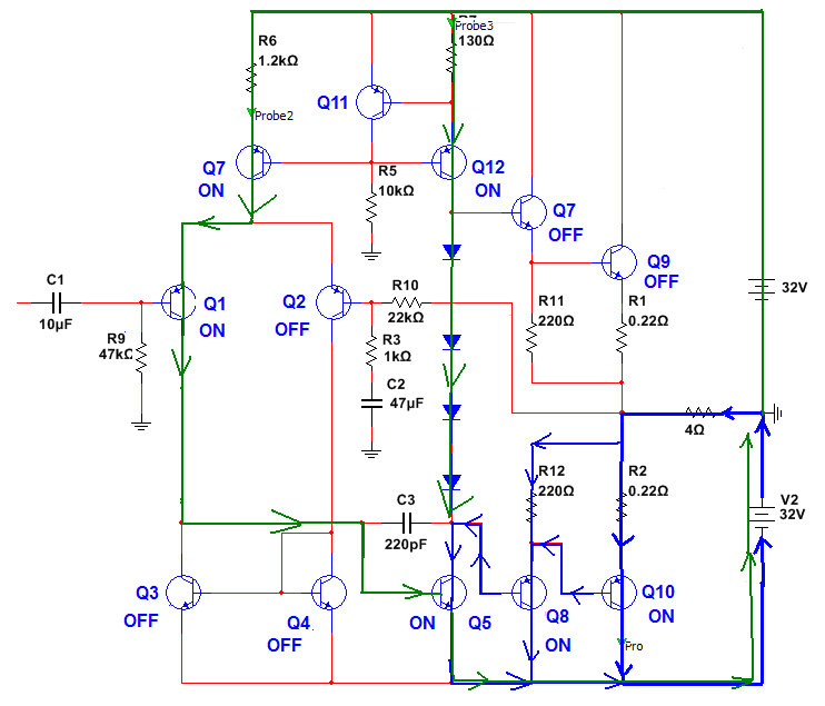
I will try to show you two extreme cases (when clipping).
For the Positive half of a sinusoidal swing:
And for Negative half of a sinusoidal swing:
This two cases should help you understand what is going on in the amplifier.
Because in the normal operation we have "slightly" similar situation.
For example:
For the Positive half, \$Q_1\$ reduce his \$I_{C1}\$ current (just a bit), hence \$Q_2\$ must increase his \$I_{C2}\$ current.
But this reduction in \$Q_1\$ current decreases the \$Q_5\$ base current also.
And all this means that the \$I_{C5}\$ collector current is decreasing also.
Hence, the voltage at \$Q_{12}\$ collector increases. The larger part of a \$Q_{12}\$ collector current (\$I_{C12}\$)can now flow into the \$Q_7\$ base. So, \$Q_7\$ and \$Q_9\$ conduct more current. And the load current increases.
I hope this helps you. Because my English vocabulary is limited.
-
\$\begingroup\$ How the current (first picture) can at Q4 collector move to Q3 collector if there is no wire between Q4 collector and Q3 collector? \$\endgroup\$– MaxMilCommented Oct 24, 2017 at 18:18
-
\$\begingroup\$ Q3 collector current discharge C3 and CbeQ5 to "quickly" Turn-OFF Q5. And this is why I have drawn this current. \$\endgroup\$– G36Commented Oct 24, 2017 at 18:21
-
\$\begingroup\$ But how Q3 can be on if Q1 is off? Q4-Q3 is current mirror and if Q4 on then Q3 also must be on \$\endgroup\$– MaxMilCommented Oct 24, 2017 at 18:24
-
\$\begingroup\$ You Answered Your Own Question. Q4-Q3 is a current mirror and if Q4 ON then Q3 also must be ON. Q3 Vbe = Q4 Vbe. Q3 is ON and is in the saturation region. \$\endgroup\$– G36Commented Oct 24, 2017 at 18:32
-
\$\begingroup\$ i. e. if there is no current through Q1 collector-emitter then Q3 can be on without any collector current because of Q4 on state? \$\endgroup\$– MaxMilCommented Oct 24, 2017 at 18:38


