How is prototyping done in a professional EE environment? Do you do your prototypes on breadboards, on copper clad boards, Manhattan style, or do you just draw schematics, order PCBs made and assembled and work with them, hacking here and there if necessary?
8 Answers
Once, about 15 years ago, I hired a new EE straight out of collage. His first day on the job, he asked me how we prototype (breadboard, wirewrap, etc.). I said that we just go directly to making a PCB, and if it works we ship it!
While I was joking, this isn't far from the truth. 90% of the products I've designed (and I've done a lot) were done this way. We decide what we want to make and then make it. Often the first version of the PCB doesn't work perfectly, so we fix it the best we can and build another round of PCB's. Then repeat this process until it works.
This same process is done for the non-electrical things too. The metal or plastic chassis, etc.
Rarely we will feel like a purely research-driven PCB is required. This is when the technology we need to invent is very difficult and we need to try it out before dedicating the resources to making an actual product. In this case we will design the PCB with R&D in mind, not volume production. This means that the parts on the PCB are spread out so they are easy to probe, and we don't care so much about the cost to make it.
In every company I've worked for this is how products have been developed. These companies were not places like Nasa that are more research-heavy.
-
\$\begingroup\$ This has been the methodology everywhere I have been as well. I would add that when designing and laying out the board test-points, debug headers, etc. is something we consciously design in to give ourselves visibility should something not work. \$\endgroup\$– MattGCommented Jun 25, 2012 at 16:50
I work for a very small company, making very small numbers of PCBs, so the way we make prototypes is probably more similar to the way David Kessner does it. We are usually very short on time and funding, so we often really need to try to get it right(ish) first time, and if it's not, then we just have to patch the boards by hand.
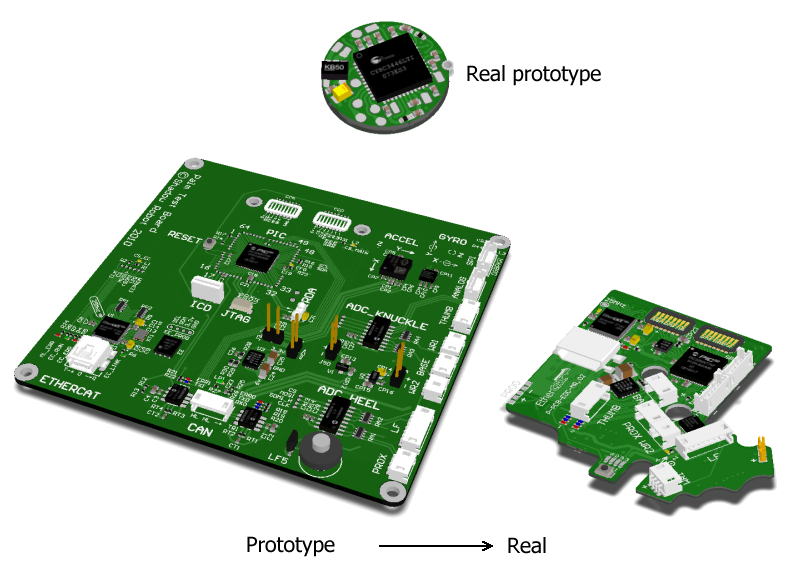
The thing that makes our PCBs unusual is that, being in robotic devices, we are always desperately pushed for space, and that space is usually a stupid shape. When I design a prototype, the question I'm trying to answer is: 'Is it feasible for these components to fit in this space?' That prototype will sometimes only exist in CAD, but I have to get most of the way through the layout before I can be sure that the design is feasible. Having done most of the design work, I'll then sneak that design onto a spare bit of space on the next PCB run we do.
For example, this little round PCB is only 15mm diameter, but has 49 components on it, and also needs space for wires to solder onto pads, for power, communication and programming. I did the layout to see if it was possible. It was, so I had one made.

Having said that, for a more complex board, it really is worth laying out a large one, for probing and scoping. This design was laid out at 100x100mm (massive!) and was invaluable for debugging. Then it was laid out on that funny shaped board which was a nightmare of physical constraints, making it hard to add debugging features. I was very glad to have had the prototype.
There is no simple "the board". A product, which may be largely a circuit board, goes thru several steps.
Most of the time I design the circuit for what we think we want the product to do, but the first version is a bench test board. This isn't even pretending to have the final mechanical form. It is a board with as much space as it takes to be able to probe around, make edits if necessary, etc. This is usually a rectangular board with rubber feet on the bottom in the corners. The circuit is what is intended for production but often with some extra debug facilities. For example, unused processor pins are brought out to labeled pads instead of just ending at the processor. There might be extra LEDs, or maybe a serial port even if the final unit won't have one. Deliberate labeled test points are added for various intermediate nets that might be useful to connect to, look at with a scope, feed a signal into, etc. There may be jumpers in a few places to disconnect parts of the circuit. The point of this board is to verify the circuit and get the basic firmware up and running.
In unusual cases when I think a circuit is risky or it's hard to know what is really needed, I may test just a small piece on one of those plug strip breadboards. For example, a while ago I had to make a product receive and process ultrasound signals, but with very low current. You can read all the datasheets there are, but for something like this it takes real experimentation to find out what gain is good enough, how little bandwidth can be gotten away with in reality, and whether some of the extra low current tricks really work as expected. Transistor datasheets generally don't tell you what the part characteristics are with only a few µA thru it. Sometimes you just have to try stuff. Fortunately that is unusual, and can be limited to a specific sub-circuit. By the way, I got the ultrasound front end amplifier down to 35 µA at 3 V quiescient current, and a gain of a few 1000 at 40 kHz, all with discrete transistors. That took some experimenting.
After the first bench test board, the customer inevitably wants something different than envisioned at first, you find little things you may want different, etc. The next version usually takes the mechanical constraints into account, so is probably a smaller more crammed board. You'd think that was it, but rarely is the second version ready to ship. That's generally not because of circuit problems, but mostly because now more people get to see it, smell it, touch it, feel it, and otherwise muck around with it. These people all have their own opinions on details of the product, and a few things will change.
The third version can sometimes be ready for production, but usually it takes one or two more revs before everyone is happy or has given in, some part got moved because the original dookicky this thing was supposed to work with got obsoleted in the two years since someone dreamed up the product idea, etc. I'd say total of 4 or 5 versions of the board is the most likely, more for large organizations that pride themselves on process and procedures.
-
\$\begingroup\$ My observation is that there is a dynamic tension between this approach and the one described by David Kessner. If you are a small company and the cost of doing yet another board spin is a significant part of overall cost, and/or if the product is relatively simple, you trend towards DK's approach. If it is a fussy product, such as described by Olin Lathrop, you probably have no choice but to do a number of spins. And yes, if the company is larger, has more resources, and is more 'ISO9000' than 'garage hacker', you may be obligated to take more steps to get to the same place, needed or not. \$\endgroup\$ Commented Jun 13, 2012 at 3:24
-
2\$\begingroup\$ @mickey: There isn't actually that much difference between what I said and what David said. He makes a bench test board less often, but other than that the process sounds pretty much the same. I should have pointed out that a bench test board is also often needed because mechanical constraints aren't known yet. Industrial design often lags electrical design. For our own products, the second rev usually ships. Also, the cost of a respin is pretty minor in the scheme of things. \$\endgroup\$ Commented Jun 13, 2012 at 12:43
In the olden days, when a small package device was an 8 pin DIL and every pin was on a 0.1" pitch then the prototyping plugboard would be wheeled out and pressed into service, tgether with some hand soldered, 3D sculpture featuring myriad components just to prove a concept.
Nowadays I tend to use the manufacturers development boards for most of the new devices that I want to try out. These all tend to have their I/O pins brought out to headers and can be wired in to other evaluation boards (microcontroller, interface devices etc) I have built up most of a new product just by joining these boards together.
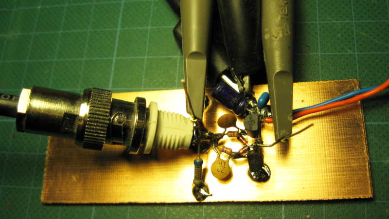
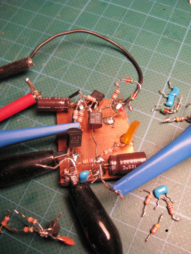
My favorite way of prototyping whenever I want to check some small details before trusting a draft or simulation and putting a small block onto an expensive multi-layer PCB with anything between 100...1000 other components:
Breadboarding. With copper-clad boards.
 Circuit is roughly similar to fig. 6 in LT's AN-104
 Source: https://electronics.stackexchange.com/a/15059/930
 This was a quick check for a voltage regulator design I needed at work and wanted to try before having a big PCB finished. It looks messy, and this is exactly the big advantage: 30 minutes in your home lab will save days of re-designing your project because you missed one tiny (and obvious?) gotcha.
... Just three tiny examples, but you get the idea. It's quick and (sometimes very) dirty, but you can keep short whatever needs to be kept short and achieve good results very fast. A very good tutorial can be found on p. 28-31 in Jim Williams' App Note 47 on the LTC website.
Of course, this will not work for BGAs and the like, but whenever I need just a tiny hack, this is my favorite way to go.
-
\$\begingroup\$ It must be nearly impossible to move it. What do you do if a colleague is developing another component and you have to test them connected to each other? \$\endgroup\$– finnwCommented Jun 13, 2012 at 21:01
-
4\$\begingroup\$ These breadboards take more abuse than one would think. One of the most beautiful examples can be found here: cds.linear.com/docs/Application%20Note/an120f.pdf \$\endgroup\$– zebonautCommented Jun 14, 2012 at 9:27
-
\$\begingroup\$ @zebonaut - Beautiful? I don't know how those people can show their face in public after that. \$\endgroup\$ Commented Jun 14, 2012 at 15:32
-
4\$\begingroup\$ @Rocketmagnet: "Those people" might care more about how their scope sees them than how the public sees them: computerhistory.org/highlights/analoglife/img/cartoons/… (cf. computerhistory.org/highlights/analoglife) \$\endgroup\$– zebonautCommented Jun 14, 2012 at 20:29
-
\$\begingroup\$ Updated link: cds.linear.com/docs/en/application-note/an120f.pdf. \$\endgroup\$– hlovdalCommented Feb 8, 2015 at 17:54
Power electronics perspective here.
The PCBs I work with are a mix of high-power noise generating components, and low-power noise-sensitive parts. Truly, the best of both worlds.
I tend to follow two paths:
If the project is based on some older work, take the older work and add-on / change things as necessary (wire in PCBs, hang parts in the air, whatever.)
If the project is totally new, and there's no way to leverage anything old, then design a new board from scratch.
Generally, if you can get away with using an existing unit as your starting point, and you already have hardware in the lab (and and as long as the changes you need to make don't end up taking longer to implement than it would to build a fresh unit) it's a tremendous time and money saver to use this as your prototype / breadboard. It can take several spins just to get the PCB "right" and this eats into your prototype debugging time. Sometime we will do a fresh build using an old design's PCBs and simply substitute parts as needed. This removes the risks inherent with a new PCB layout.
Whenever we need to design a new PCB, we try to achieve fit/form/function as closely as possible to the end requirement - even for the first spin. Just in case things work perfectly (ha!). PCB spins take time and resources, so we closely scrutinize every board so that they have the best chance of 'working' (or 'working better than before') every time we do a spin. Continuous improvement, so to speak.
If I feel that it is necessary (or schedule-advantageous) to have a partial prototype before the first PCB version, I tend to create it by combining evaluation boards for the technologies involved, or stand-ins for them. For example, a micro-controller board might get a hand-wired SPI interface connecting it to an FPGA board, or perhaps a wiring harness is created to bit-bang some module from a PC parallel port (often using what is on its way to becoming the device firmware, only with a different low-level I/O wrapper).
Once you have a product line started, PCB's from existing versions of the product (or even a product from a different line that uses some of the same technology) can often be used as a prototyping platform. That can mean anything from simply trying out new firmware, to using them with eval boards, or making a little adapter to replace one chip, or even just using the PCB with all but one component removed, as a breakout board for that chip.
While if pursued to far it can easily become a distraction, there can at times be a use for an in-house capability to make simple PC boards on the order of carriers for particular ICs or small circuits to add additional functionality (or correct oversights). I've worked places that did this with milling/laser resources that were required for special purpose RF boards, which we sometimes leveraged for small logic modules. For personal projects, a small toner-transfer single sided SMT board can be produced in one hour and assembled in a second - it's not the quality of a quick turn PCB house, but quick-turn does not mean same-day circuit operation. I'll sometimes send the file to the board house and then make my own version to keep the project moving.
Typically, the Chinese factories we work with make the prototypes for us, then we will make modifications to them to fix problems, add features, etc. Then they make another prototype with our changes, we test that revision, find that they missed something, or our improvements caused other problems, etc. and repeat the cycle of modifications until it works well enough to sell. (Note that I did not say "works perfectly"...) Sometimes the changes we make involve breadboards, but usually they're just components hanging in space soldered to each other just sturdily enough to prove that it works.
I can only think of a few times when I actually built most of the prototype on a solderless breadboard first, and even then, some of the things plugged into the breadboard were small circuit boards of their own, either eval boards made by the chip manufacturer or other boards I had lying around that I could cut into, because the chips are impossible to use with a breadboard on their own.
