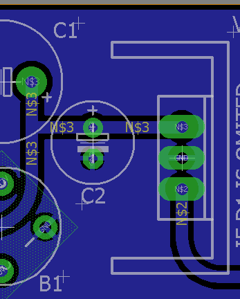
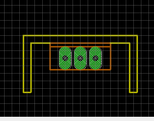
I am using Eagle version 8.4.0 and I am having a problem with a component that I edited where my ground fill is overlapping the pads. The component is an LM78xx from the Sparkfun library. I changed the shape of the pads from round to long and rotated them 90°. When I updated my schematic/board the changes show up but the polygon fill for the ground plane did not change. I saved everything, closed and reopen the project and even deleted and recreated the polygon. It still has the overlap. I have made similar edits to other components on the same board, just changing the size of the pad--not the shape, and they work fine. Someone please tell me what I am missing... and thank you.
3 Answers
I'd suggest you add a KeepOut layer. It goes by the name of tRestrict (for top layer) and bRestrict (for bottom layer). It's the same as polygon pour but it prevents any other wire/polygon to be routed within that Restrict(ed) area.
Place it and do ratsnest!
-
\$\begingroup\$ Thank you. The keepout took care of it. I would still like to know why that was necessary, but it is good enough that it works! \$\endgroup\$– MennesetCommented Nov 2, 2017 at 4:32
-
\$\begingroup\$ Actually, I had forgotten that I had created another polygon over each of the pads which forced a gap in the underlying GND polygon. The keepout actually had no discernable effect. Thank you though. \$\endgroup\$– MennesetCommented Nov 2, 2017 at 5:09
-
\$\begingroup\$ (fyi the problem with the second polygon is that it left some orphaned bits next to the pad that I just didn't like.) \$\endgroup\$– MennesetCommented Nov 2, 2017 at 5:23
Neither of the suggested answers were able to solve my issue. I managed a workaround... I created a short trace under the pad, the length of the pad with a width of 1.92mm. This provided a gap which is almost perfect. I still would like to understand the issue and why it is a problem in the first place. As an additional test, I created an entirely new component using the long pads and it has the same problem.


