1
\$\begingroup\$

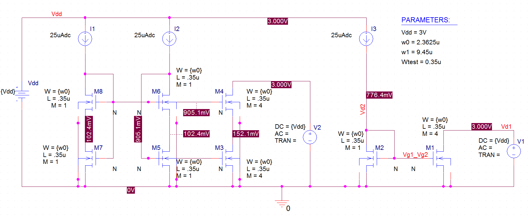
I'm working on designing a cascode current mirror, depicted below:

Schematic for circuit in question

Constraints: all Von needs to be above 200 mV, all Vds neds to be at least double Von, L is 0.35 um.

Derived from the SPICE file, k' = 181.47 uA/V^2, and the given bias current is 25 uA. Rearranging the equation for Von to solve for W gives:

$$ W=(2I_{D}L)/(k'(V_{ON})^2) $$

I input my given values and find a value for W of 2.41 um. To make them have a slightly happier ratio, I bump that down to 2.3625 um, which makes W/L 6.75.

I then make all of my Ws that value, run a bias simulation, and investigate; this is what I find. All voltages are in mV (I apologize, there seems to be no way to make a table):

MOS - Vgs - Vth - Von - Vds - Region

M1 --- 776 - 585 - 191 - 3000 - Saturation

M2 --- 776 - 558 - 218 - 776 - Saturation

M3 --- 905 - 585 - 320 - 152 - Triode

M4 --- 905 - 585 - 320 - 2850 - Saturation

M5 --- 776 - 582 - 194 - 102 - Triode

M6 --- 803 - 587 - 216 - 803 - Saturation

M7 --- 905 - 582 - 323 - 102 - Triode

M8 --- 803 - 587 - 216 - 803 - Saturation

Ignoring for a moment M1 and M4, why are M3, M5, and M7 in triode? I've tried changing the W up and down, and I can't get any of those Vds values to go above 200, let alone 400 mV. How do I set my Vds higher? What's wrong with the Von of M3, M4, and M7?

\$\endgroup\$
2
  • \$\begingroup\$ Triode means Vds < Vgs - Vth. M3/5/7 all have their gates connected to points which are higher than their drains by at least Vth. Easiest to analyze is M7. For M8 to pass 25uA its Vgs must be >Vth. So M7's gate voltage must be equal to its drain voltage plus Vgs(M8). Why would you expect them to be in saturation? \$\endgroup\$
    – τεκ
    Commented Jan 12, 2018 at 22:18
  • \$\begingroup\$ Uhh...faulty assumption, maybe? I was assuming that, with the circuit working properly, each transistor would be operating in saturation...is that not the case? \$\endgroup\$
    – John Doe
    Commented Jan 12, 2018 at 23:07

2 Answers 2

0
\$\begingroup\$

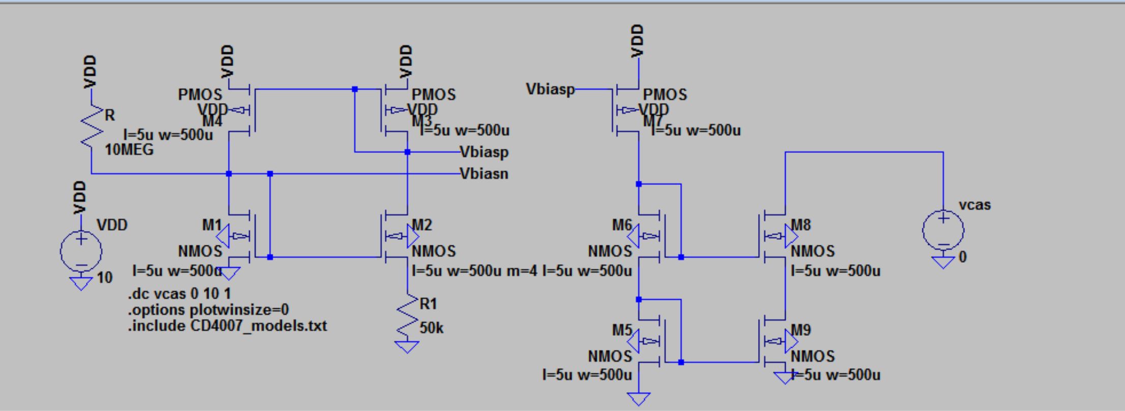
you don't have a bias, therefore an incomplete current mirror, so electrically it will act as a class A stage with a ccsenter image description here

Stick a resistor in where Ibias would be so you can bias the bottom fets

Here is another example:

enter image description here

I recommend you look at this guy's page, since you are learning the circuit: http://cmosedu.com/jbaker/courses/ee420L/s17/students/garrod/Lab%209/Lab%209.htm

\$\endgroup\$
4
  • \$\begingroup\$ I'm not sure this is correct. My textbook's example of a wide-swing cascode current mirror is precisely as I have it depicted here (minus the simple current mirror to the right, I thought that I didn't include that; oh well), and it has no resistors. \$\endgroup\$
    – John Doe
    Commented Jan 12, 2018 at 23:04
  • \$\begingroup\$ you have to understand textbook schematics are not always how they are made, especially if it is explaining things like current flow, so they use simplified schematics. \$\endgroup\$
    – drtechno
    Commented Jan 12, 2018 at 23:10
  • \$\begingroup\$ Granted, but it seems like the differences would be for noise and/or error reduction, not completely changing the function of the circuit. In the textbook in question (Analysis and Design of Analog Integrated Circuits, Gray et. al, 4th Ed.), it does mention that M7 only serves to bias the source of M8, and they can be collapsed into one, but I didn't realize that that meant that it would be in triode. Additionally, I'm not sure where I would place the resistor based on the schematic you provided. \$\endgroup\$
    – John Doe
    Commented Jan 12, 2018 at 23:40
  • \$\begingroup\$ its another simplified schematic. \$\endgroup\$
    – drtechno
    Commented Jan 12, 2018 at 23:45
0
\$\begingroup\$

@τεκ Thank you for helping to correct my false assumption.

From Analysis and Design of Analog Integrated Circuits, Gray et. al, 4th Ed., pp. 270-271 (emphasis added):

In a single combined input branch, some element must provide a voltage drop equal to the desired difference between the gate voltages of M1 and M2...This voltage difference can be developed across the drain to the source of a transistor deliberately operated in the triode region...Since M6 is diode connected, it operates in the active region as long as the input current and threshold are positive. However, since the gate-source voltage of M6 is equal to the gate-drain voltage of M5, a channel exists at the drain of M5 when it exists at the source of M6. In other words, M6 forces M5 to operate in the triode region.

\$\endgroup\$

Your Answer

By clicking “Post Your Answer”, you agree to our terms of service and acknowledge you have read our privacy policy.

Not the answer you're looking for? Browse other questions tagged or ask your own question.