3
\$\begingroup\$

This question is somewhat relevant to this one. However I am sure it well deserves to be separate.

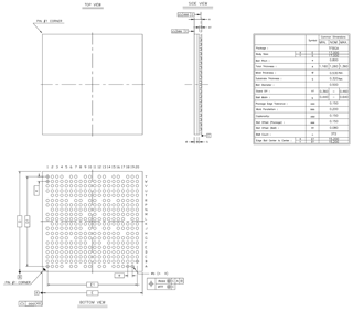
I created a custom device/symbol/footprint for an ARM MCU. However I am doubtful whether I created a footprint correctly. The MCU documentation defines dimensions as below:

Package documentation

When I was defining pads I used SMD pad with 100% roundness and 0.5x0.5mm size. Which resulted in below output (layers visible are top, tStop and tCream). Which looks like it won't be possible to send even a single trace between the balls (due to tStop size):

Package footprint sample

Now, my understand is that traditionally there is enough space left between balls for at least a single copper trace, which does not look like it is happening from above picture.

My question: Did I read/understand package dimensions from the documentation correctly? Did I define the pad size correctly? Or it should be smaller? In other words, what is the proper way to define footprint of the BGA device using Eagle?

UPDATE: Found this document which obviously applies mostly to TI chips, but there is a section of "Standard BGA", which I think should be very useful. It shows different sizes (including ball landing size etc).

\$\endgroup\$
2
  • \$\begingroup\$ Not an answer, but you may find this to be an interesting read on the challenges of working with BGA on a budget: hforsten.com/making-embedded-linux-computer.html \$\endgroup\$
    – Daniel
    Commented Jan 13, 2018 at 9:06
  • \$\begingroup\$ @DanielGiesbrecht thanks. That is definitely going to be very useful! \$\endgroup\$ Commented Jan 13, 2018 at 9:10

2 Answers 2

2
\$\begingroup\$

For BGA packages, you typically want the stop mask to be either slightly smaller (mask defined pad) or a tiny bit larger (copper defined pad) than the copper pad.

Eagle will automatically make the stop mask larger than the pad by a specific percentage set in the DRC of the board. This is usually much larger than you would want for a BGA.

I would advise that you disable the Stop and Cream options in the pad properties for each pad, and then manually draw a circle with a width of 0 (i.e. filled) on each of the tStop and tCream layers. This way you have full control over how bit the circles are.

The datasheet should give details of how big the mask and cream/stencil circles should be.


As a side note, for a 0.8mm pitch BGA, you may or may not be able to route between the pads, though you probably can get a single trace through the gap. Typically when wiring BGAs, you escape route them by placing a small via diagonally from the pad (not in the pad!). That way you can route the traces out on other layers.

\$\endgroup\$
9
  • \$\begingroup\$ Right, the specifications document I got does not have anything about pad size. I suspect it might be in another document (that the specifications references, called "Hardware design guide") from the same manufacturer, however that document is N/A. So I am trying to figure out sizes with what I have. Might try to find any existing library with similar ball size and see there I guess. \$\endgroup\$ Commented Jan 13, 2018 at 9:12
  • \$\begingroup\$ @AlexKey what's the part number for the MCU? \$\endgroup\$ Commented Jan 13, 2018 at 9:31
  • \$\begingroup\$ It’s Marvell’s 88F6828 \$\endgroup\$ Commented Jan 13, 2018 at 9:33
  • \$\begingroup\$ Contact Marvell's support - this document may be restricted. \$\endgroup\$
    – Anonymous
    Commented Jan 13, 2018 at 11:58
  • \$\begingroup\$ @Anonymous would wonder why though, the HW specifications and other related documents went to unrestricted access some time ago and that document would still stay restricted? I tried to contact them as a matter of fact, and no one get back to me (for several times) \$\endgroup\$ Commented Jan 13, 2018 at 13:09
2
\$\begingroup\$

Thanks to @TomCarpenter advises (and my research) I have found information that I was looking for.

First (and primary) relevant document is a TI wiki page that provides tables at the bottom pf this answer. According to those tables for BGA with pitch of 0.8mm and ball diameter 0.5mm the following applies:

  1. Nominal landing diameter (copper pad size) = 0.4mm ± 0.05mm
  2. via copper (outer) diameter = 18mil (~0.45mm)
  3. via drill size = 10-8mil (~0.254-0.2mm)
  4. copper trace width = 4-5mil (~0.1-0.127mm)
  5. Clearance width = 4mil (~0.1mm)

Second found document produced by IPC supposedly has more detailed information on these number, however the document is paywalled and therefore is N/A.

Third document that was found comes from JEDEC and provides very detailed information on each measure that is seen on dimensions picture in the question. In this document in table 4.27-2 it provides a b1 dimension for ball diameter 0.50mm equal 0.35mm. According to description this is the size of opening in resistant layer that would expose copper pad for soldering with the ball (or in other words this is the minimum size of the copper pad).

Since JEDEC document provided minimum size but no upper boundary, I would consider using numbers from TI document. Using those sizes in Eagle package editor and enabling Cream and Stop on the pads I get following picture:
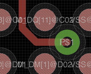
BGA routing between pads and with vias

Which looks like normal routing with default values of stop bounds should work just fine. Worth noting that with these sizes default value of stop bounds is equal to the one recommended by TI (4mil or 0.1mm).

Relevant tables from TI page:

IPC-7351A for NSMD Pads

Nominal            Land    Nominal  Land
Ball     Reduction Pattern Land     Variation
Diameter           Density Diameter

0.75        25%       A      0.55   0.60-0.50
0.65        25%       A      0.50   0.55-0.45
0.6         25%       A      0.45   0.50-0.40
0.55        25%       A      0.40   0.45-0.35
0.5         20%       B      0.40   0.45-0.35  
0.45        20%       B      0.35   0.40-0.30
0.4         20%       B      0.30   0.35-0.25
0.35        20%       B      0.30   0.35-0.25
0.3         20%       B      0.25   0.25-0.20
0.25        20%       B      0.20   0.20-0.17
0.2         15%       C      0.17   0.20-0.14
0.17        15%       C      0.15   0.18-0.12
0.15        15%       C      0.13   0.15-0.10


PCB Typical Feature Sizes For Standard (non-Via Channel) BGA Arrays

Ball         Via        Via Hole  Trace    Clearance  Micro
Pitch        Diameter     Size    Size                Vias?

0.8mm pitch   18 mil    10-8 mil  4-5 mil     4 mil    No
0.65mm pitch  16 mil*   8 mil*    4 mil*      4 mil*   No
              12 mil    6 mil     4 mil       4 mil    Yes
0.5mm pitch   10 mil    5 mil     3 mil       3 mil    Yes
0.4mm pitch   10-8 mil  5-4 mil   3 mil       3 mil    Yes

*16 mil diameter/8 mil hole vias are only possible if done in 
 a creative way that puts traces only in between every other via.
 In other words, 16/8 vias, when placed between the balls, will 
 move enough to allow one 4 mil trace per pair, but not one 4 mil 
 trace per via, so for some designs like the DM365 and DM355, 
 16/8 mil vias should be possible in your application since there 
 are some areas to place vias in the array.  However for Freon, 
 since it's a full array, it is not possible to use 16/8 vias 
 unless only every other pin is used (not likely).  16/8 vias are 
 uncommon in the PCB fab world, but some companies can do them 
 without micro vias.
\$\endgroup\$

Your Answer

By clicking “Post Your Answer”, you agree to our terms of service and acknowledge you have read our privacy policy.

Not the answer you're looking for? Browse other questions tagged or ask your own question.