1
\$\begingroup\$

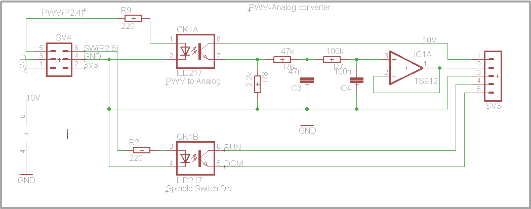
I am trying to understand how the circuit shown below works. It converts a PWM signal to a 1-10V analog signal. The circuit is from this link.

I want to understand how it works because I want to design a circuit that controls a LED driver (such as this one for example) using an analog signal 1-10v. I have several questions:

  1. The operational amplifier is configured as a voltage follower. In the schematic, its supply voltage is not specified. To guarantee that the operational amplifier can provide a 10 V output, should it have a supply voltage of more than 10V?
  2. The voltage at R8 is at least 9.6 V (when the optocoupler drives, it is in saturation, Ic=10mA). What is the correct way to dimension the low pass filter so that a duty cycle of 10% corresponds to 1V, 20% to 2V, etc?
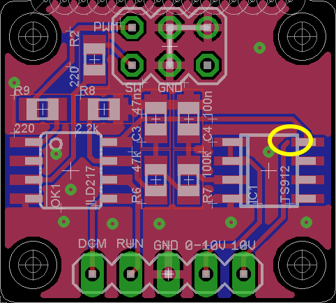
  3. I am also looking at the layout and would not it be necessary to connect the track that I marked in the image?

Thanks.

Schematic

PCB layout

\$\endgroup\$
8
  • 2
    \$\begingroup\$ Where are the schematic and PCB layout from? Didn't it come from a site with explanation? Trying to make sense out of google image found schematics almost never makes sense. \$\endgroup\$
    – PlasmaHH
    Commented Jan 16, 2018 at 10:07
  • 2
    \$\begingroup\$ Trying to maintain an accurate PWM duty cycle through an opto coupler is always going to end in tears. The design is flawed. \$\endgroup\$
    – Andy aka
    Commented Jan 16, 2018 at 10:11
  • 1
    \$\begingroup\$ The supply voltage on the op-amp is given; it is 10V across pins 4/8 in the lower left of the schematic. \$\endgroup\$ Commented Jan 16, 2018 at 10:21
  • 1
    \$\begingroup\$ @Andyaka depending on the application, a software compensation for the design's inherent non-linearity could do the job, it will never be a very good DAC, but it does work. \$\endgroup\$
    – Sclrx
    Commented Jan 16, 2018 at 10:34
  • 1
    \$\begingroup\$ And how will that compensate temperature variations? I'm not talking about basic non-linearity. @Sclrx you don't need to answer this. \$\endgroup\$
    – Andy aka
    Commented Jan 16, 2018 at 10:40

2 Answers 2

4
\$\begingroup\$
  1. From your OP-Amp Datasheet, we know that the output can go from (VCC-)+300 mV to (VCC+)-400mV, so for this application, i would supply 12V to your OpAmp.
  2. The exact value is not that critical, you just need to design it so the cutoff frequency is well below your PWM frequency, but not too low to avoid lowering your DAC max bandwith
  3. Yes it should be connected. But however, this layout is very problematic, no decoupling/filtering whatsoever, i would redo the whole thing.

But if i were to be honest, my advice would be to redesign your own DAC, it is not that difficult, and you could easily achieve better results than with this thing you have here.

\$\endgroup\$
2
  • \$\begingroup\$ Thanks Sclrx. How would you improve the layout? \$\endgroup\$ Commented Jan 17, 2018 at 15:37
  • \$\begingroup\$ @FranMartin Add decoupling on your couplers supply, and filter out HF in parallel with the diodes, but this deserves its own question. And as i said, if you need to change something, you might as well change the whole design. \$\endgroup\$
    – Sclrx
    Commented Jan 18, 2018 at 8:41
-1
\$\begingroup\$

A few points; the 10v goes nowhere on the board, bad layout. The opto isolator is not isolating, the grounds are common. Solution is to separate the grounds, still works. The op amp really needs a 12v supply to get full range 0 to 10 volts. This does actually work on the simulator.

\$\endgroup\$
1
  • 3
    \$\begingroup\$ Wow, no need to shout. Please edit your post to be in decent grammer. Also this does not really seem to be an answer to the (already answered) question... \$\endgroup\$
    – jusaca
    Commented Aug 2, 2019 at 7:16

Your Answer

By clicking “Post Your Answer”, you agree to our terms of service and acknowledge you have read our privacy policy.

Not the answer you're looking for? Browse other questions tagged or ask your own question.