1
\$\begingroup\$

There are already many questions about proper placement of decoupling caps in different situations (multiple layers, different sides etc).

As a general rule of thumb (e.g. How to place decoupling capacitor in four-layer PCB?), it is frequently recommended to directly connect the decoupling caps between the IC pins and from there a via to power/ground plane. The reason is to ensure that the currents flow through the cap.

Based on this Decoupling cap: Closer to chip but with via or farther without via? and this How important is it to put decoupling caps on the same side of the PCB? question I have decided to to put my caps at the opposite side. Furthermore, I will have an 8 layer board with multiple ground planes/power planes.

In order to connect my decoupling caps I have a forest of vias from the VDD pin to the other side of the board. On the other side, I connect the caps between the ground paddle and the vias.

However, in order to follow the rule of thumb above, I should not connect the vias to the ground plane. Instead, use separate vias to connect the cap to the supply plane.

This seems quite wasteful and odd to me. To make the long question short:

When placing decoupling cap at the other side of the board, is it ok to connect the power/ground planes with the same vias that connect the cap and the chip or should they be separately connected?

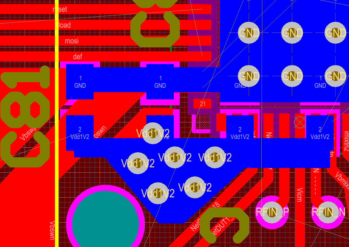
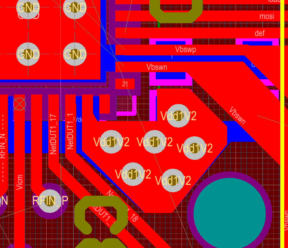
In order to give a precice example, this shows front and back layout:

Front Back

As can be seen, the 6 vias labeled Vdd1V2 also connect to the power plane Vdd1V2 directly. I do not have separate vias to connect the (then local) Vdd1v2 network on the back to the power plane.

\$\endgroup\$
2
  • 1
    \$\begingroup\$ I cropped the image from the other post to only include the cap you refer too. You can roll it back if you think its an inappropriate edit. Ideally, you would post some examples of the possibilities you are referring to, to avoid misunderstandings. \$\endgroup\$
    – Wesley Lee
    Commented Feb 2, 2018 at 1:27
  • \$\begingroup\$ It looks like the decoupling caps go to "Vdd1V2" and "GND" Vias, which then connect to the internal power planes, and finally the IC pins. Won't that spoil the decoupling? I thought the proper sequence was: Power Plane VDD -> Via -> Decoupling Cap+ -> IC VDD Pin, and respectively Power Plane GND ->Via -> Decoupling Cap- -> IC GND Pin. Basically force the IC to draw from the caps before drawing from the power planes. \$\endgroup\$ Commented Oct 21, 2022 at 23:28

2 Answers 2

2
\$\begingroup\$

I hate rules of thumb, I abolish them wherever I work. It's far better to understand why. With that said your goal in a good decoupling strategy should be to minimize the impedance across your frequencies of interest. This translates into wanting to minimize inductance which usually means reducing the loop area or reducing the impedance of the connecting traces/planes/vias. So you can create a nice low inductance path between your chip pins and that cap by placing them on the same layer and running wide traces to it.

Then you want a nice low inductance path to your power planes. One set of vias right at the cap seem like a nice idea. Two sets of vias would of course lower your inductance further since the inductance of each via would be in parallel with each other. (I often do Via in pad but I have the luxury of using those processes. You may too if you're already at an eight layer board).

So with that said and you being a designer who understands your system you can now make your own tradeoffs. In your structure above it looks to me like your loop area is unnecessarily long so I would look for ways to reduce it. But maybe you have other reasons for that so just keep in mind that you want to reduce the loop area and impedance between the caps, pins and the power planes.

If you want to know if what you've done is "good enough" or even more difficult optimal before you build it you will have to understand your dynamic current requirements and then do some level of simulation. Otherwise your options are really to try it, or over design it a bit to give yourself some margin.

\$\endgroup\$
1
  • \$\begingroup\$ I think you misunderstood my question. The picture should only support my question - it was taken from somewhere else. It is specifically about leaving the VDD connection local and connecting to the power plane afterwards vs. not. I updated the question with my own layout. I hope it's more clear now. \$\endgroup\$
    – divB
    Commented Feb 2, 2018 at 7:45
1
\$\begingroup\$

The lowest inductance for connecting a bypass capacitor has TWO requirements: 1) lowest enclosed area 2) lowest inductance from the silicon bondwires out thru the leadframe out to the bypass cap.

(1) might be accomplished with cap on the backside, under the (adjacent?) VDD/RTN pair of the MCU

(2) might be accomplished using PLANES under the IC VDD/RTN pins and having the same plane under leads to the bypass cap and that same plane under the bypass cap.

\$\endgroup\$
1
  • \$\begingroup\$ I think you misunderstood my question. When connecting the VDD pin with the cap - that forms a local network. Now I can connect it to the supply in the middle of this local network or after the cap. As I understand from my referenced posts, the latter is usually preferred (it isolates the cap better from the supply). But when I use vias to place it at the bottom and these vias connect to power plane I automatically have the first option. I updated my question and hope it is more clear now. \$\endgroup\$
    – divB
    Commented Feb 2, 2018 at 7:50

Your Answer

By clicking “Post Your Answer”, you agree to our terms of service and acknowledge you have read our privacy policy.

Not the answer you're looking for? Browse other questions tagged or ask your own question.