2
\$\begingroup\$

TL:DR How do I know how to size transistors?

This is the same problem as this one.

Now knowing that I can change L, I know that my W/L ratio to make Von = 200 mV is roughly 6.75. Also knowing that M5 is supposed to be operating in triode, here's my thought process:

Von > 200 mV; this is set by W/L = 6.75 (math done elsewhere).

Vds (for devices operating in saturation) > 2Von (= 400 mV)

Vd5 = 400 mV

Which means that Vd5 = 800 mV

Which means that Vg5 = 800 mV

Therefore Vth <= (less than or equal to) 600 mV.

Assuming that Vth are relatively similar:

Vgs6 = Vg6 - Vs6 = Von + Vth

Vg6 = Von + Vth + Vs6

Vg6 = 200 mV + 600 mV + 400 mV = 1.2v = Vg8 = Vd8 = Vg7.

The maximum that Vs8 can be is 800 mV for M8 to meet the Vds spec. However, since Vgs7 = 1.2 V and Vth = 0.6 V, then:

Vds7 < Vgs7 - Vth = 600 mV.

And that's where my train of thought stops. The only pertinent equations for MOSFETs that I can think of involve W/L, not one or the other, so I don't know how to set the sizes of these transistors. I was told that M5, M6, and M8 should all be the same size, and the Gray et. al. book Analysis and design of Analog integrated circuits says that W/L7 should be 1/3 of the other W/L's, but I don't know if that's meant for unity gain current mirrors or all current mirrors in this configuration.

If I don't want to keep that ratio that I calculated earlier...then I'm really lost and don't know where to begin.

I'm trying to figure out how to find out as much as possible from hand calculations before I go to simulation. I've got a lot of different knobs to turn: W7, L7, M7, W8 = W5 = W6, L8 = L5 = L6, M8 = M5 = M6 (multiplier factor, not transistors themselves). The smallest number of knobs I can turn (if M8, M5, and M6 are identical and I keep the initial calculated ratio AND if the ratio of M7 is supposed to be 1/3 of the others) is 4; that number quickly gets out of hand if I started changing them relative to each other.

What's the next step? How do I size these transistors?

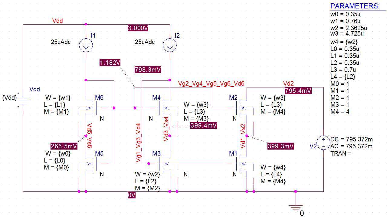
Edit: Walking through simulations. Will be updated periodically

2018 Feb 18

L1,3,5,6 = 0.35 µm

L2&4 = 0.7 µm

W1&3 = 2.3625 µm

W2&4 = 4.725 µm

W5 = 0.35 µm

W6 = 0.76 µm

M1-2 = 4

M3-6 = 1

Final Schematic

V2 = 795.3 mV sets the output current equal to 100 µA, and the bias voltages are as follows:

-------------------------M1 ---- M2 ----- M3 ---- M4 ---- M5 --- M6

Vgs (mV) ---------- 798.3 --- 782.7 --- 798 --- 783 --- 1182 -- 917

Vth (mV) ----------- 571 ----- 558 ---- 571 --- 558 --- 385 --- 480

Von(mV) ----------- 227.3 --- 227.8 --- 227 --- 225 --- 797 --- 488.5

Vds (mV) ----------- 399.3 --- 396 ----- 399 --- 399 --- 266 --- 917

Vds % Difference - -0.17% - -1.01% - -0.25% - -0.25% -- N/A -- N/A

Ro = 2 M-Ohm (Can't get the Greek letter to display).

Still, no matter what I do, Vd4 is constant at less than 800 mV. What sets this level? Is it M5?

\$\endgroup\$
4
  • \$\begingroup\$ Would you please filter out all of your speculations and stick to the math. Your wall of text is impossible to follow. End questions with a '?'. \$\endgroup\$
    – user105652
    Commented Feb 8, 2018 at 2:02
  • \$\begingroup\$ Do these designs allow for FETS with various thresholds (Vts) caused by very short channel or longer channel? \$\endgroup\$ Commented Feb 8, 2018 at 3:24
  • \$\begingroup\$ @analogsystemsrf um... yes? I have no idea. Incidentally, in that schematic, I've got all the bulks tied to vss; I've since connected them all to their respective sources. \$\endgroup\$
    – John Doe
    Commented Feb 8, 2018 at 3:32
  • \$\begingroup\$ You aren't really clear in your objective here (or I'm missing it in your description). What is your overall goal you want to achieve? Is it to get vd4 at a different voltage than 800mv? I'm doubting that. Given that i2 above is fixed, I would expect changing m3 w and or l, would have some effect on the vd4. \$\endgroup\$
    – pat
    Commented Dec 14, 2021 at 4:16

1 Answer 1

0
\$\begingroup\$

Sizing depends on what you want to achieve. You may aim for the specific output resistance, for the specific voltage swing etc. Once you have it, you turn on Monte Carlo to see if the current matching is acceptable.

In your example here you make make L longer for M3 while rather keeping the minimum length of M4. Additionally, M4 will be rather wide, as it is biased from more or less diode-connected voltage, but must still keep the drain of M3 on a useful voltage level.

\$\endgroup\$
15
  • \$\begingroup\$ I'm not even at the point where I can decide what I want to achieve because I can't get all of the transistors biased in the right spot. Either Von is too low for one or more transistors or Vds is too low for one or more transistors. No matter what I've tried, I haven't been able to properly bias the three transistors meant to be in saturation. \$\endgroup\$
    – John Doe
    Commented Feb 8, 2018 at 14:08
  • \$\begingroup\$ @John Doe To make it clear: we are talking about this schematic and the three transistors in question are M5, M6, M7? You rather won't get a clear saturation for these transistors due to the architecture, that is, the way how they are connected. M8, M6 and M4 should be very wide and short. M3 and M5 can be longer, but will be rather wide. \$\endgroup\$
    – Tako
    Commented Feb 8, 2018 at 21:41
  • \$\begingroup\$ That is the schematic in question, and those are the transistors in question. When you say wife and short, or wide and long, I've never done this before, so I have no concept of what that means. All I have that is the least bit definite is a W/L ratio. Past that, I'm stumped. \$\endgroup\$
    – John Doe
    Commented Feb 8, 2018 at 22:05
  • \$\begingroup\$ @John Doe The best would be to run the simulator and work on it step by step. I understand that you are simulating this circuit? If so, please share the results in your question. We will work on it point by point. \$\endgroup\$
    – Tako
    Commented Feb 9, 2018 at 8:46
  • \$\begingroup\$ I've added the simulation results from my most recent attempt. \$\endgroup\$
    – John Doe
    Commented Feb 9, 2018 at 17:32

Your Answer

By clicking “Post Your Answer”, you agree to our terms of service and acknowledge you have read our privacy policy.

Not the answer you're looking for? Browse other questions tagged or ask your own question.