0
\$\begingroup\$

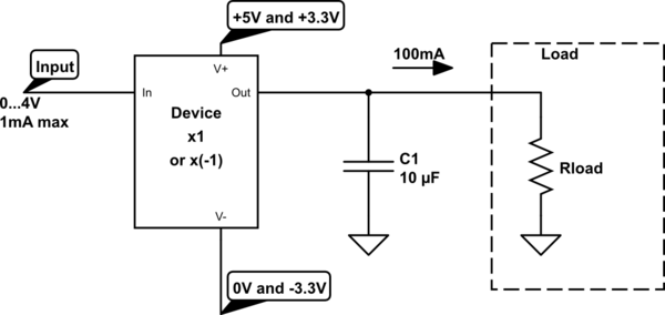
I am trying to solve the following problem which - until today - I thought to be a trivial one: I have multiple reference voltages (from different sources) that I need to buffer and/or invert, filter with a large cap (10uF) and needing to supply around 100mA to the load:
schematic

simulate this circuit – Schematic created using CircuitLab

The input references range from 0V to 4V and the supplies should be either single supply +5V (for the buffers) and +/-3.3V dual supply (for the inverting ones). Furthermore, it should be two opamps per chip.

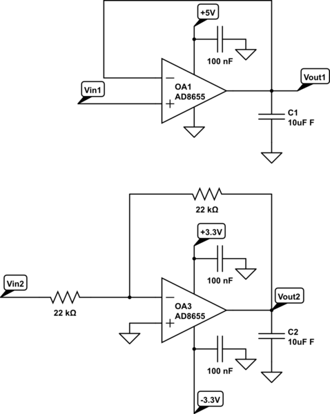
The canonical solution to the problem is using an op-amp in (a) unity gain configuration (b) inverting amplifier:
schematic

simulate this circuit

I wasted my whole day finding the right opamp. There are many that can drive arbitrary caps (I do not want to deal too much with compensation networks) and there are many that can supply >100mA. But the intersection is zero.

For example, the AD8655 provides +/-220mA but drive max. 500pF (and that rings already). The ADA4807 is stable for CL>100nF without compensation but the output current is limited to about 50mA. Many op amps are explicitely built to be stable for all capacitive loads, like the AD826 but again, current too low.

Am I missing something?

\$\endgroup\$
9
  • 1
    \$\begingroup\$ Why do you expect a capacitor on the output of the op-amp to filter the signal? If the op-amp is ideal its output is like an ideal voltage source, and the capacitor provides no filtering. If the op-amp is not ideal, as you know the capacitor just causes the op-amp to ring. \$\endgroup\$
    – The Photon
    Commented Feb 9, 2018 at 5:49
  • 1
    \$\begingroup\$ If you want to filter the signal, filter the control signal, then buffer it to provide the required load current. If you want to minimize voltage variation due to changing load current, just make sure to use an op-amp with adequate bandwidth to handle the load variations. \$\endgroup\$
    – The Photon
    Commented Feb 9, 2018 at 5:51
  • \$\begingroup\$ It is common practice so filter voltages with 10uF or so. Just as an example: ti.com/lit/an/slyt355/slyt355.pdf \$\endgroup\$
    – divB
    Commented Feb 9, 2018 at 5:51
  • \$\begingroup\$ The reference (REF50) in that note is likely designed specifically to use the output capacitance to improve stability rather than to reduce it. They might draw an op-am in its block diagram but it doesn't behave like an op-amp you buy as a discrete part. \$\endgroup\$
    – The Photon
    Commented Feb 9, 2018 at 5:55
  • 1
    \$\begingroup\$ In any case, my advice is trust your op-amp and control loop to do its job. If you need to handle fast load current changes, simulate your design to find output impedance and adjust to keep it low in the frequency range you need. Adding 10 uF shunt capacitors is likely counter-productive, unless perhaps you have a long trace between the op-amp and the load (in which case the trace inductance can decouple the capacitor from the op-amp and save you from instability problems) \$\endgroup\$
    – The Photon
    Commented Feb 9, 2018 at 6:18

2 Answers 2

3
\$\begingroup\$

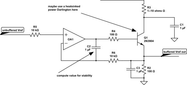
Here is one approach

schematic

simulate this circuit – Schematic created using CircuitLab

The massive capacitance [I used at least 10uF] on emitter of the output buffer causes phase shifts and BODE plot rolloff and likely instability; including R6 (to isolate) opamp (-)pin from the emitter, and including C2 (needed to provide a look-ahead on the phase shift) provides a control-loop "zero".

In my original implementation, we used bipolar-input-device opamps with the inevitable input bias currents; by making R5 = R6, the nominal voltage drops are cancelled and the temperature-dependent deltaIbias/deltaTemperature error is reduced, to zero if the two input transistors of the opamp's diffpair are indeed matched.

R3 and C1 provide high frequency filtering of incoming power trash; the control-loop performs well at low frequencies. I knew the end-user-system was a high-sample-rate video imager and the focal-plane diodes have ZERO ability to reject power-supply-noise; system raw power were Switching Regulators at high-chopping frequency for efficiency, and I selected R1 and C1 to provide 20 to 40 dB additionally filtering at the SwitchReg chopping frequency.

Result of including R3/C1? There were no herringbone beatnotes on the display video screen, even with system gain turned up (via SPI) to the 8X max value. To delight of the program manager, we did achieve the 17 nanoVolts/rtHz noise floor. The pixels were quiet.

\$\endgroup\$
1
  • \$\begingroup\$ Thank you, this is very helpful! I meanwhile came up with something fairly similar but without R5, C2, R6, R3, C1. As OA1 I use LT1819, R4=400, C3=10uF, R2=22k//Rload, Q1=MBT6429DW1T1G. In LTspice this seems to work. Would you be able to elaborate the need&purpose of the other components and how you came up with the values? (If possible I would avoid to change my layout too much now). \$\endgroup\$
    – divB
    Commented Feb 12, 2018 at 8:29
1
\$\begingroup\$

A voltage regulator is basically voltage reference + error amplifier + pass transistor, with the error amplifier compensated correctly to work with driving (through the pass transistor) a lot of capacitance.

\$\endgroup\$

Your Answer

By clicking “Post Your Answer”, you agree to our terms of service and acknowledge you have read our privacy policy.

Not the answer you're looking for? Browse other questions tagged or ask your own question.