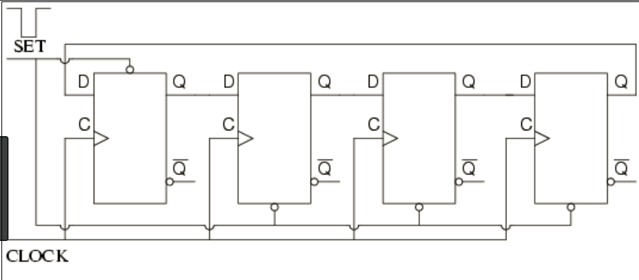
This is an effort to find the rise and fall time of the following circuit.
I have calculated the rise time and requesting confirmation from expert’s end. There are some assumed values like trace impedance parasitic capacitance, kindly note that is for the sake of calculation purpose. I am much interested how the calculations need to be done than the numerical values. But values can be updated if it is not at all close to real values.
See the details, D Flip-flop (SN74LVC1G80) is powered with 3.3 V and logic levels are 0 V (Logic LOW) and 3.3 V (logic high).
Assumed parasitic capacitance = 3 pF
Assumed trace impedance = 10 Ohm
Data switching at a rate of 500 kHz
Following method used to calculate the rise time:
\begin{align} 3.3 \cdot 0.1 &= 3.3 \left(1- e^{-\frac{t_1}{RC}}\right) &\implies t1 &= 3.1608\text{ ps}\\ 3.3 \cdot 0.9 &= 3.3 \left(1- e ^{-\frac{t_2}{RC}}\right) &\implies t2 &= 69.078\text{ ps} \end{align} So the net rise time is = 69.078 – 3.1608 = 65.9172 ps
Observations
- Rise and fall time is independent of the data signal switching frequency
- Rise or fall time can be increased by adding series resistor and parallel capacitor to the each output stage of the FF ( that is pin Q ).
Kindly confirm or point out my mistakes.

