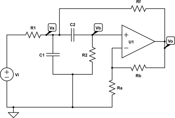
I'm trying to understand the transfer function of the band pass sallen key filter, which looks like:
With the following circuit:
How can I analyse it to get the transfer function? Thanks for any help.
I'm trying to understand the transfer function of the band pass sallen key filter, which looks like:
With the following circuit:
How can I analyse it to get the transfer function? Thanks for any help.
You can use modified nodal analysis to solve for all unknown node voltages and unknown currents. Once you get the node voltage, you can find the transfer function. For the analysis, I denote node and current as in the picture below.
Now you can write KCL for every node and a constraint by OpAmp.
You can get 7 equations:
Then you can solve 7 equations to get all unknown voltages and unknown currents. Finally transfer function is just V5/V1.
General hints (works not only for this particular configuration):
Do following steps in \$s\$-domain:
You can use symbolical math tools, e.g. sympy package for Python, Maple, Mathematica...
Here is a python script doing the algebra (using sympy); not sure though if correct:
# deriving the transfer function of a Sallen-Key band pass filter

from sympy import Symbol, symbols, solve, collect

s = Symbol('s')

def Xc(C): global s; return 1 / (s * C)

Vin, Vout, Vaux = symbols('Vin Vout Vaux')
R1, R2, C1, C2, Rf, Ra, Rb = symbols('R1 R2 C1 C2 Rf Ra Rb')
X1, X2 = Xc(C1), Xc(C2)

# get expression for Vaux by solving KCL in node_aux:
Vaux_expression = solve(    (Vin  - Vaux) / R1
                          + (Vout - Vaux) / Rf
                                  - Vaux  / X1
                                  - Vaux  / (X2 + R2),
                        Vaux)[0]

Vpos = Vaux_expression * R2 / (X2 + R2) # voltage at pos. input of OpAmp
Vneg = Vout * Ra / (Ra + Rb)            # voltage at neg. input of OpAmp

# get expression for Vout by solving equation Vneg = Vpos for Vout
Vout_expression = solve(Vpos - Vneg, Vout)[0]

# get transfer function H(s) by defining formula:
H = Vout_expression / Vin
H = collect(H, s)
print H
Result:
C2*R2*Rf*s*(Ra + Rb)/(C1*C2*R1*R2*Ra*Rf*s**2 + R1*Ra + Ra*Rf + s*(C1*R1*Ra*Rf - C2*R1*R2*Rb + C2*R1*Ra*Rf + C2*R2*Ra*Rf))
This filter can be analyzed using the fast analytical circuits techniques or FACTs. The principle is to determine the time constants of the circuit in two different configurations: when the excitation is reduced to 0 V and with a nulled output when the excitation is back.
Reducing the excitation to 0 V, means replacing the input source \$V_{in}\$ by a short circuit. Then, "look" at the resistance \$R\$ offered by the energy-storing elements (the caps) to form time constants, \$\tau_1=RC_1\$ and \$\tau_2=RC_2\$. The below drawings illustrate this principle:
Using these two drawings, you determine the following time constants:
\$\tau_1=C_1(R_1||R_f)\$
\$\tau_2=C_2(\frac{k_1(R_1R_2+R_1R_f+R_2R_f)-R_1R_2}{k_1(R_1+R_f)})\$
\$b_1=\tau_1+\tau_2\$
Then, you set capacitor 1 in its high-frequency state (a short circuit) and determine the resistance \$R\$ looking into \$C_2\$'s terminals:
You have \$\tau_{12}=C_2R_2\$ and \$b_2=\tau_1\tau_{12}\$
Finally, you determine the gain \$H^2\$ when capacitor \$C_2\$ is a short circuit:
The complete transfer function is determined according to \$H(s)=\frac{sH^2\tau_2}{1+sb_1+s^2b_2}\$
However, even if this expression is mathematically correct, you have zero insight on the plateau gain \$H_{MB}\$ and the tuning frequency which are truly the design goals. You need to rework the formula according to the following low-entropy format: \$H(s)=H_{MB}\frac{1}{1+(\frac{\omega_0}{s}+\frac{s}{\omega_0})Q}\$. This is what the following Mathcad sheets show and compare the various responses:
So the point is not just write a transfer function linking \$V_{out}\$ to \$V_{in}\$ but more rearranging the result in a meaningful form from which you gain insight and can design for a certain goal in tuning frequency and quality factor: this is all what FACTs are all about.
There are really only two nodes that need exercising. All others are defined by node b. The input node node is defined by the input voltage source.

simulate this circuit – Schematic created using CircuitLab
From a comment:>My algebra is pretty good. But I do not understand the way to proceed to end up with the transfer function.
Node a: Apply KCL.
$$\left(\frac{1}{R_{1}}+\frac{1}{R_{f}}+C_{1}s+C_{2}s\right)V_{a}(s)-\frac{1}{R_{f}}V_{o}(s)-C_{2}sV_{b}(s)=\frac{1}{R_{1}}V_{i}(s)\tag{1}$$
Node b: Apply KCL.
$$\left(\frac{1}{R_{2}}+C_{2}s\right)V_{b}(s)=C_{2}sV_{a}(s)$$
Solve for \$V_{a}\$
$$\left(\frac{1}{R_{2}C_{2}s}+1\right)V_{b}(s)=V_{a}(s)\tag{2}$$
Substitute (2) into (1)
$$\left(\frac{1}{R_{1}}+\frac{1}{R_{f}}+C_{1}s+C_{2}s\right)\left(\frac{1}{R_{2}C_{2}s}+1\right)V_{b}(s)-\frac{1}{R_{f}}V_{o}(s)-C_{2}sV_{b}(s)=\frac{1}{R_{1}}V_{i}(s)\tag{3}$$
From a comment:>but I do not know how to derive the equations for v+ and v−
Let \$K=1+\frac{R_{b}}{R_{a}}\$. Then, \$V_{o}(s)=KV_{b}(s)\$. Substitute into (3).
Notice that \$v-=v+=v_{b}\$
$$\left(\frac{1}{R_{1}}+\frac{1}{R_{f}}+C_{1}s+C_{2}s\right)\left(\frac{1}{R_{2}C_{2}s}+1\right)V_{o}(s)-\frac{K}{R_{f}}V_{o}(s)-C_{2}sV_{o}(s)=\frac{K}{R_{1}}V_{i}(s)\tag{4}$$
I leave the algebra to you to simplify into the form shown in the OP.