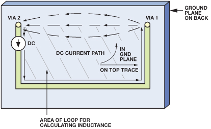
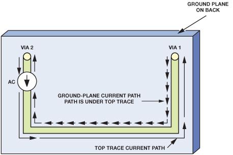
The theory says that the current return path at high frequency is on the reference plane right under(or above) the signal trace.
I know it is true and I have always assumed it was, but I would like to understand it properly.
My trouble is about it can be power or gnd plane for the reference plane.
If we use a 6 layer stackup:
Signal
GND Plane
Signal
Signal
PWR plane
Signal
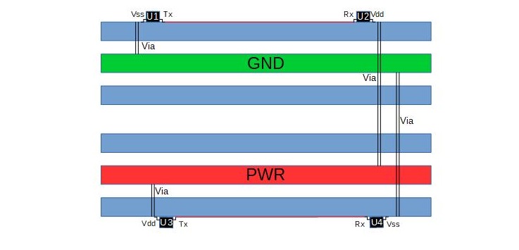
If we take the example of two device U3 and U4 on Bottom layer (referenced to a Vdd power plan), with U3 having a Tx pin connected to a Rx pin on U4: When U3 output a 1 the current goes:
Power Vdd=>U3 Vdd pin=>U3 Tx pin=> U4 Rx Pin=> U4 Vss Pin=> and then?
How is the current passing from U4 Vss pin to Vdd power plan? Capacitor? Because there is no connection as you can see in the picture/
Also wy is the current not flowing to the GND plan? Is the inductance created by going to the GND Plan that much bigger than the one created by going to the Vdd Plan?
Now if we take the same example but on Top layer( referenced to a ground plane):
When U1 output a 0 am I right to assume the current goes:
Power Gnd=>U1 Vss pin=>U1 Tx pin=> U2 Rx Pin=> U2 VddPin=> again and then?
How is the current passing from U2 Vdd pin to Gnd power plan? Capacitor?
Also why is the current not flowing to the Vdd plan? Is the inductance created by going to the Vdd Plan that much bigger than the one created by going to the Vdd Plan?
Another question related to the answer is, what if the reference power plane is not of the same voltage as U1 and U2 power voltage? Is that still working as a power reference plane?
Edit:
Here is a drawing of the stack up and components I am talking about for clarification:


