3
\$\begingroup\$

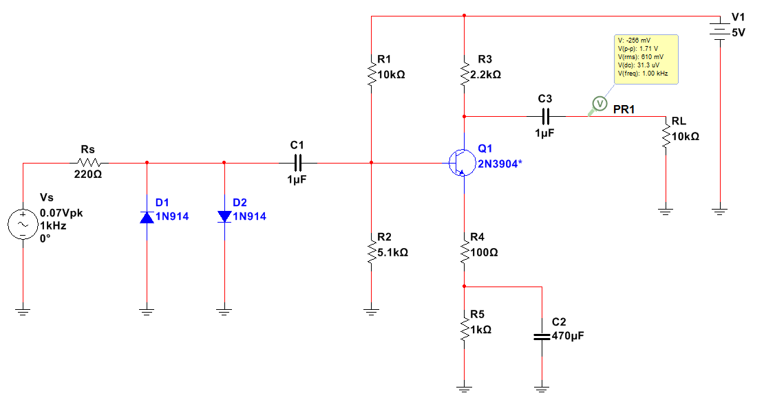
I am calculating the voltage output of the below circuit. The output I have calculated varies by 0.1 of a volt compared with the simulation I created using multisim, but I am not certain this is correct.

The questions I have:

  1. Are the below calculations correct?
  2. How do I display the results in decibels
  3. What is the ouput voltage with no load?

Thank You.

Values:

$$Vs=70mV_{peak}$$ $$2n9304\beta = 100$$

DC Analysis:

$$V_B=Vcc.(R2/(R2+R1))=1.689V $$ $$V_E=V_B-0.7V=0.989V$$ $$I_E=(V_E/(R4+R5))=0.899mA$$ $$V_C=VCC.(IC*R3)=3.022V$$ $$RE=(V_T/I_E)=(23mV/0.899mA)=25.584\Omega$$

AC Analysis (Voltage Gain):

$$Av_{no load}=V_{out}/V_{in}=((R3*IC)/((RE+R4)*IE)=(2.2k\Omega/125.584)=17.518 $$

$$Z_{in}=(R1||R2)||(Z_{INQ})$$

$$Z_{INQ}=V_{in}/I_{in}=(125.584*I_E)/I_B=12683.984\Omega$$

$$Z_{in}=2667.24$$

$$OutputVoltage=V_s*(Z_{in}/(Z_{in}*Rs)*Av_{no load}*(RL/(RL+R3)$$

$$OutputVoltage=0.929_p=1.857_{p-p}$$

enter image description here

\$\endgroup\$
3
  • \$\begingroup\$ Owen I used my rules-of-thumb and found no big differences between my mental model and your work. Be aware the Zin will vary with frequency, especially at high frequencies where the Cob (C_base_collector) will demand large amounts of charge from the signal noise; 1mV on base becomes 17mV on collector, the net deltaV being 18mV and both base(your signal source) and the collector nodes must provide this displacement current/charge. \$\endgroup\$ Commented Mar 25, 2018 at 21:45
  • \$\begingroup\$ What is your noise floor? The biasing may have some effect, but a very low Zsource will obviate those resistors. The unavoidable Noise come from R4 (100 ohm) at 4nV/3.1 = 1.3 nanoVolts RMS per squareroot of your bandwidth, and the likely similar-values rbb' (aka base-spreading resistance) which is the resistance in the silicon material from the base-contact-bond-wire down and under into the actual base-region between emitter and collector. If equal, total Vnoise will be 1.414 * 1.3 = 1.8 nanoVoltsRMS. In 100KHz bandwidth, input-referred-noise is 1.8 * 310 = 500 nanoVolts RMS. After 17X, ??? \$\endgroup\$ Commented Mar 25, 2018 at 21:51
  • \$\begingroup\$ I get \$V_B=1.66\:\text{V}\$ on a cursory calculation that takes into account the base current load on the divider. \$\endgroup\$
    – jonk
    Commented Mar 25, 2018 at 23:38

2 Answers 2

1
\$\begingroup\$

You know, for the base resistor divider pair, that \$V_\text{TH}=V_1\frac{R_2}{R_1+R_2}\$ and that \$R_\text{TH}=\frac{R_1\,\cdot\, R_2}{R_1+R_2}\$. From this, KVL yields:

$$V_\text{TH}-R_\text{TH}\cdot I_\text{B}-V_\text{BE}-\left(\beta+1\right)I_\text{B}\cdot\left(R_4+R_5\right)=0\:\text{V}$$

Solving the above for \$I_\text{B}\$ (unless you say otherwise, I'll assume you can plug in values and compute it) you can then find that:

$$V_\text{B}=V_\text{TH}-R_\text{TH}\cdot I_\text{B}$$

The value you get from the above is not \$V_\text{B}\approx 1.689\:\text{V}\$. It is more like \$V_\text{B}\approx 1.658\:\text{V}\$, taking your assumption \$V_\text{BE}=700\:\text{mV}\$ and \$\beta=100\$. (That's only a \$30\:\text{mV}\$ difference. But since we are calculating values using formulas, we should arrive at the same figure.) So \$V_\text{E}\approx 0.958\:\text{V}\$ and \$I_\text{E}\approx 871\:\mu\text{A}\$. So \$r_e\approx 29.86\:\Omega\$.

So far, though, we haven't considered the input signal attenuation. Before going further, it might be a good time to go back and do that. With your input capacitance at \$1\:\mu\text{F}\$ and \$f=1\:\text{kHz}\$, I find \$X_{\text{C}_1}\approx 159.2\:\Omega\$. \$C_1\$ and \$R_\text{S}\$ are in quadrature to each other, so the source impedance works out to about \$272\:\Omega\$. The load seen by your source will come from the base divider pair and the BJT's base load, or \$R_\text{IN}=R_1\mid\mid R_2\mid\mid \left(\beta+1\right)\cdot R_4\$. This is about \$2.525\:\text{k}\Omega\$ and it suggests that the input will be attenuated down to about 90% of the source magnitude. This needs to be accounted for in your estimate of the total gain.

Discounting any load and also the Early Effect, this means \$\mid\, A_v\mid \approx 90\%\frac{R_3}{R_4+r_e}\frac{\beta}{\beta+1}\approx 15.1\$. If you now add in the \$10\:\text{k}\Omega\$ load, the output is attenuated to another \$\approx \frac{10\:\text{k}\Omega}{10\:\text{k}\Omega+2.2\:\text{k}\Omega}\approx 82\%\$, or down to \$\mid\, A_v\mid \approx 12.4\$.

I'm holding short of providing detailed answers to every nuance in your questions, for now. I think you can work with what I've provided here to reach them on your own. However, one note. You should be able to find, literally everywhere on the web, the formula for decibels given a voltage ratio: \$20\log_{10} \mid\frac{v_{out}}{v_{in}}\mid\,=20\log_{10} \mid A_v\,\mid\$. You should be able to easily calculate that value for both unloaded and loaded cases.

\$\endgroup\$
0
\$\begingroup\$

Gain with no load = -R3/(re + R4)

= -2.2K/(25.6 + 100) = -17.5

Gain with 10K load added = -(R3//RL)/(re + R4)

= -(2.2K//10K)/(25.6+100) = -14.36

In practice the circuit gains will be a little less than those calculated above because the bypass capacitor,C2 has some reactance at signal frequencies. That is to say there will be some ripple on this capacitor.

Zin = R1//R2//(hFE * (R4+re))

Also, multisim uses some other factors in collector current formulas. Firstly, they consider V_CE which can not be neglected. Also there are other factors such as base - collector resistance which affects the collector current also. Multisim also considers parasitic capacitance forming in the depletion layers which again affect collector current and the the small signal analysis for gain calculation.

\$\endgroup\$

Your Answer

By clicking “Post Your Answer”, you agree to our terms of service and acknowledge you have read our privacy policy.

Not the answer you're looking for? Browse other questions tagged or ask your own question.