1
\$\begingroup\$

I am studying Transistors from the book: Arts of Electronics by Paul Horowitz and Winfield Hill (second edition). I have a few questions related to the working of a transistor, especially in the saturation region.

In the rule 1, as to the working a transistor, it has been mentioned: "The collector must be more positive than the emitter".

1. Why is that so?

2. And is it true only for that forward-active region or in all regions (i.e. saturation, cutoff, reverse-active)?

3. Also what would happen if the collector potential becomes less than that of the emitter potential?

Another query that I have is, 'does saturation imply a maximum value of current through the transistor? Or is the maximum value of current achieved before the device enters the saturation region (which I believe should be the case)?'

Edit: While reading a similar question on the website, I was directed to the link: Transistors in saturation region where a user (Studiot), explained the saturation from the perspective of an electronic engineer, he mentioned that the collector voltage can not be zero (or less than the emitter voltage, which is grounded in his circuit). Hence the saturation voltage can be around 0.2V - 0.4V.

Also I read that in the saturation region, it appears as if the emitter and collector are short-circuited, then why is there still a potential difference of 0.2V - 0.4V existing?

\$\endgroup\$
2
  • \$\begingroup\$ The emitter and collector of a transistor can be swapped, and the device will still act like a transistor, but most parameters will be severely degraded. Saturation is when both base-collector and base-emitter junctions are forward biased. \$\endgroup\$
    – user57037
    Commented Apr 1, 2018 at 16:43
  • \$\begingroup\$ There are quite a few questions regarding material from the book mentioned. Would it be helpful to have a tag for it? \$\endgroup\$ Commented Apr 16, 2019 at 15:48

1 Answer 1

2
\$\begingroup\$

Although the question shows lack of research ( near duplicate ) , I'll offer some sage advice.

  1. Collector is more positive for NPN and negative inverse or complement for PNP. It ( the NPN) MUST be more positive to have any current gain such that when Vbe is always forward biased but Vce>0 , the transistor has current gain >10% of its max hFE. Vbc must be negative or Collector higher than bas and emitter to achive rated hFE. Usually for linear sin swing you must have Vce>1 for low current and >2V for high current and higher linearity but as a switch Vce<<1V ideally and as you were told, typ. 0.2 to 0.5 for selected suitable parts.

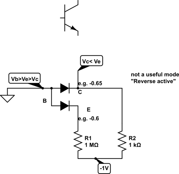
  2. Yes except in reverse active limited to low voltage, hFE~1 is not used.

  3. if Vce=-ve for NPN it implies both BC and BC are forward biased relative to the base and merely act as small signal diodes.

schematic

simulate this circuit – Schematic created using CircuitLab

Because of doping differences. BE is not the same as BC in VI characteristics yet on a DMM this is how you determine is a transistor is NPN or PNP by testing the forward voltage at 0.1mA ~0.65V in "Diode test mode"

Although this is an over-simplistic explanation , when a transistor is in saturation mode rated at Vce(sat) @Imax with Ic/Ib=10 the higher doped BE diode has a higher ESR which dominates the Vce @Ic. The effective Rce or collector emitter resistance as a switch ( or ESR as I generalize as) is the incremental ΔVce/ΔIc rise when pulling down a load current.

Vce may start from low mV with pA to 0.2V nominal ( at some rated current) to >1V under high pulsed current above rated steady-state current.

This Rce value (aka "BJT switch resistance between collector emittor) is rarely shown in datasheets except for Diodes Inc and a few others as "low Rce" switches. It costs more , but performs better and in general always is inverse to power rating of the part.

\$\endgroup\$
5
  • \$\begingroup\$ I am sorry if the question seems non-serious. I did a lot of work on it :( The main issue I am facing is why should the collector potential be more positive than the emitter potential? Also in the 3. point of your answer you have BC twice, please correct that \$\endgroup\$ Commented Apr 1, 2018 at 16:25
  • 1
    \$\begingroup\$ @ means "at" some specified value \$\endgroup\$
    – D.A.S.
    Commented Apr 1, 2018 at 16:35
  • \$\begingroup\$ Ok. In your answer what does @ signify? Also you mentioned both BC and BC in your third point shouldn't it be BE and BC? \$\endgroup\$ Commented Apr 1, 2018 at 16:38
  • \$\begingroup\$ And in reverse active mode shouldn't the EBJ and BCJ be reverse biased? \$\endgroup\$ Commented Apr 1, 2018 at 16:40
  • 1
    \$\begingroup\$ No: > "active" means conducting meaning forward biased and since BJT's have BC normally reverse biased or Vc>Vb for NPN and reverse for PNP Therefore "reverse active" is not the voltage but reverse to normal operation. or Reverse active: poor β; not useful; β<=1 \$\endgroup\$
    – D.A.S.
    Commented Apr 1, 2018 at 16:44

Your Answer

By clicking “Post Your Answer”, you agree to our terms of service and acknowledge you have read our privacy policy.

Not the answer you're looking for? Browse other questions tagged or ask your own question.