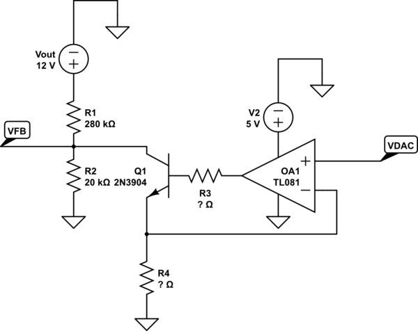
The TL081 used in OP diagram does not work at all in this application unless you can supply it with at least +/- 5V. LM358 or LM2904 are much better choices.
If you really have your heart set to using this circuit, you're overthinking it. Whatever your opamp positive node sees is what it tries to adjust the transistor emitter to produce by adjusting the base current.
So figure out what you'd like your output voltage adjustment range to be and set the emitter resistor to a suitable level WRT min/max output from DAC.
You basically have a maximum incoming current from R1, \${12V \over 280k} = 43µA\$ (if R2 is shorted) that will be split between R2 and R4. You max voltage is with R2 and R4 in parallel (transistor active) and your min voltage is R2 alone (Transistor switched off).
43 microamps is very very small, consider scaling the resistors to e.g. 14k and 1k. Note that this will mess your feedback loop if you don't adjust capacitors to match, which is beyond the scope here. But the same scaling factor applies, in this case you'd want a 20x larger compensation capacitor to keep the pole frequency. Other figures will work out as well of course. Whatever part value is convenient.
A worked out example
It's not immediately obvious how to deal with the relationships so I'll go over these for you. This is career-advancing stuff. We'll work this out from bottom to top.
I'll keep the 20k + 280k voltage divisor here and use 20k as R4.
If we denote transistor current as \$I_{Q1}\$, the relationship between the DAC and the transistor current is \$I_{Q1} = {V_{DAC} \over R4}\$.
We're ignoring the base current here. In normal operation the base
current should be about 1% of the collector current i.e. not matter
much. However, when you drive the circuit out of range the base
current will start "lifting" the R4 voltage
The reference voltage for the SMPS is \$V_{ref}={12V * 20k \over (280k+20k)} = 0.8V\$
This should be found in datasheet, I just put in the values from the circuit diagram.
Since we know the current flowing through the transistor and the reference voltage at the top of the transistor, it's easy enough to calculate series resistance of Q1 and R4.
\$R_{Q1}+R_{R4}={V_{ref} \over I_{Q1}}=R_{bias}\$
Armed with relationship from the \$V_{DAC}\$ to \$R_{bias}\$ it becomes rather easy to work out relationship from \$V_{DAC}\$ to \$U_{out}\$, keeping in mind \$R_{bias}\$ is in parallel with R2 for the reference voltage division.
I'll leave working out the figures how to do that for the reader.
When when \$V_{DAC}\$ rises high enough, \$R_{bias}\$ becomes less
than \$R4\$ and as negative resistors were sold out, this is
not possible. With a transistor this is masked by the bias current,
with mosfet the gate voltage will go to max. The maximum usable current is \$ V_{ref}\over R4\$
So as an example, 0.3V \$V_{DAC}\$ results in effective bias resistor of 53.3k. This then will adjust output voltage to 16.2V.
A second homework assignment is to adjust R2 and R4 to produce different output voltage ranges.
Usable output voltage range with 20k R2 and R4.


