Alright! I got it. I think it's a dirty, dirty (but clever, in my humble opinion) hack that I'd never use in a real design. Use at your own
risk!

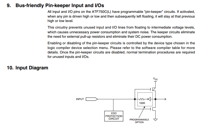
from the ATF750C datasheet, it proclaims that there is a bus hold feature.
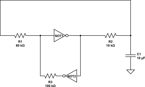
The bus hold feature is basically a positive feedback path with 100K of series impedance. If you put an inverter as the "normal" digital path, then by using both, you basically get a negative feedback path and a positive feedback path.
When you have positive feedback, you can use it to create a Schmitt trigger, and if you have negative feedback, you can create an RC oscillator--therefore you can make a Schmitt trigger RC oscillator.

simulate this circuit – Schematic created using CircuitLab
NOT1 is the regular inverter, and NOT2 is part of the bus hold inverter. Adjust R2 and C1 to meet your timing needs.
Please note this still puts the input in undefined state for a long time (which causes shoot through current), so I'd highly advise against this.
I checked the datasheet and there doesn't seem to be any slew rate constraints, but if there is and they just forgot to write it, this circuit may destroy your CPLD, so be careful.
Bottom line is, since it's a CPLD, it hints me that this is not a hobby project. If this is for commercial use, please don't use this hack; go for a 555 timer or a small Schmitt trigger (it's cheap, and I'm sure you can get it in SOT5 or something tiny like that).
EDIT:
If you wanna go for the Schmitt trigger route, I found some single, 5V Vcc Schmitt triggers in 5TSSOP (tiny) packages for like <15 cents each @ 100qty. View this question to get how to set the frequency:
How to delay a "not gate oscillator" to make it run at a desired frequency?


