First Question:
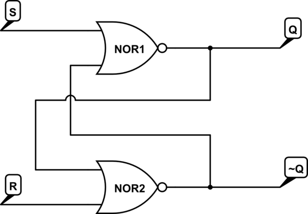
It is merely a convention. Let us consider the case where the input to NOR gates are S NOR ~Q and R NOR Q.

simulate this circuit – Schematic created using CircuitLab
When (S,R) pair is (1,0) then Q is 0 and ~Q is 1. Changing S,R to 0,0 causes no change in Q, ~Q values. When S,R is further changed to 0,1 then Q and ~Q change to 1 and 0 respectively. And then changing S,R to 0,0 again causes no change in Q or ~Q values. The basic functioning of the latch remains same. The conventions are as the way you stated just because setting S,R to 1,0 would also set Q,~Q to 1,0. The point of conventions are to make sure everything has the same meaning for everyone. Nevertheless, it is a good practice to put schematics of the simplest things like latches just to make sure in case of any discrepancy, people can refer to the architecture and conventions you have used.
Second Question:
Again, it is just a convention, nothing to worry about too much if you understand the latches and can explain the transitions. NAND gate based SR latches are actually called S'R' latches. This is because unlike NOR gate based SR latch which require a 1 to set or reset, NAND based gates required 0. There is nothing sacrosanct about the convention used, your convention is equally good. Just make sure that you provide a truth table or schematic as per your design and nomenclature.
If you still have doubts, I recommend the small section on SR latches in the book by Morris Mano, Chapter on Synchronous Sequential Logic.

