2
\$\begingroup\$

There are many similar questions but I didn't really find the answer I want.

I have many 2-layer boards for analogue-audio-stuff. I use both layers for routing and I have ground fills on just one layer. (mostly on bottom layer). Well it works this way but..

Why shouldn't I fill also the other layer with ground copper and connect them using multiple small stitches/vias? That would reduce the impedance between some grounding components which were connected through narrow ground paths on one layer.
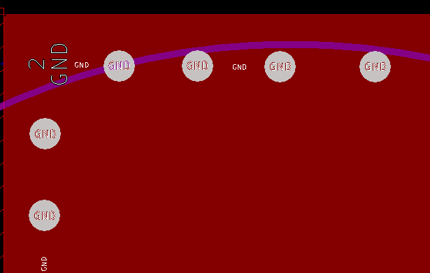
(Image source: forum.kicad.info)

Do you see any reasons not to fill the both layers with ground?

\$\endgroup\$
2
  • 1
    \$\begingroup\$ We do that routinely...I don't see any issue. Be sure they're connected thoroughly, though, or they can become antennas. \$\endgroup\$ Commented Jun 8, 2018 at 15:43
  • 1
    \$\begingroup\$ Yeah. It is very often done. Could even be considered a best practice. Just make sure you look over the gerbers to make sure design rule clearances didn't create any copper islands or too-thin slivers of copper between vias or pins. \$\endgroup\$
    – user57037
    Commented Jun 9, 2018 at 8:32

4 Answers 4

2
\$\begingroup\$

If this is for Audio I wouldn't think impedance performance of the ground plane matters that much. However it may help to have the pour on both sides because you are more likely to have a shorter ground return path.

If you have gone through your single ground plane and verified that there is plenty of return path for the amount of current being consumed, you should be fine.

There is no reason not to fill both planes.

\$\endgroup\$
2
\$\begingroup\$

You can pour power supply (or supplies with a split plane or polygon pours) on the other side too.

Either way, be sure you're not coupling noise from ground or power supply currents from power back to low level circuits.

\$\endgroup\$
2
\$\begingroup\$

What your really doing is increasing the capacitance between the traces on the top and the ground plane that is filled on the top. So if your design can tolerate a tiny amount of capacitance (you can calculate plane to plane capacitance, since the tool only accepts one width, use the smaller of the two, which will most likely be the plane size). Most likely this capacitance will be a few pF's.

The only other caveat is if the current from what ever source you have on the top plane is going to the bottom plane through the vias, then you have a small amount of inductance in the nH range which will be parallel inductance for each via.

This would create a filter most likely in the range of GHz and above, so it probably doesn't apply to an audio design and the effects of the small parasitics will be negligible. If you were doing something above 100MHz or transmission lines generally is where you start to worry about these effects.

\$\endgroup\$
1
\$\begingroup\$

Fill located near sensitive traces will tend to shield the trace against Electric Field interference, because the Fill copper will grab some of the Efield flux lines, and you may be 3 to 10 dB lower interference.

\$\endgroup\$

Your Answer

By clicking “Post Your Answer”, you agree to our terms of service and acknowledge you have read our privacy policy.

Not the answer you're looking for? Browse other questions tagged or ask your own question.