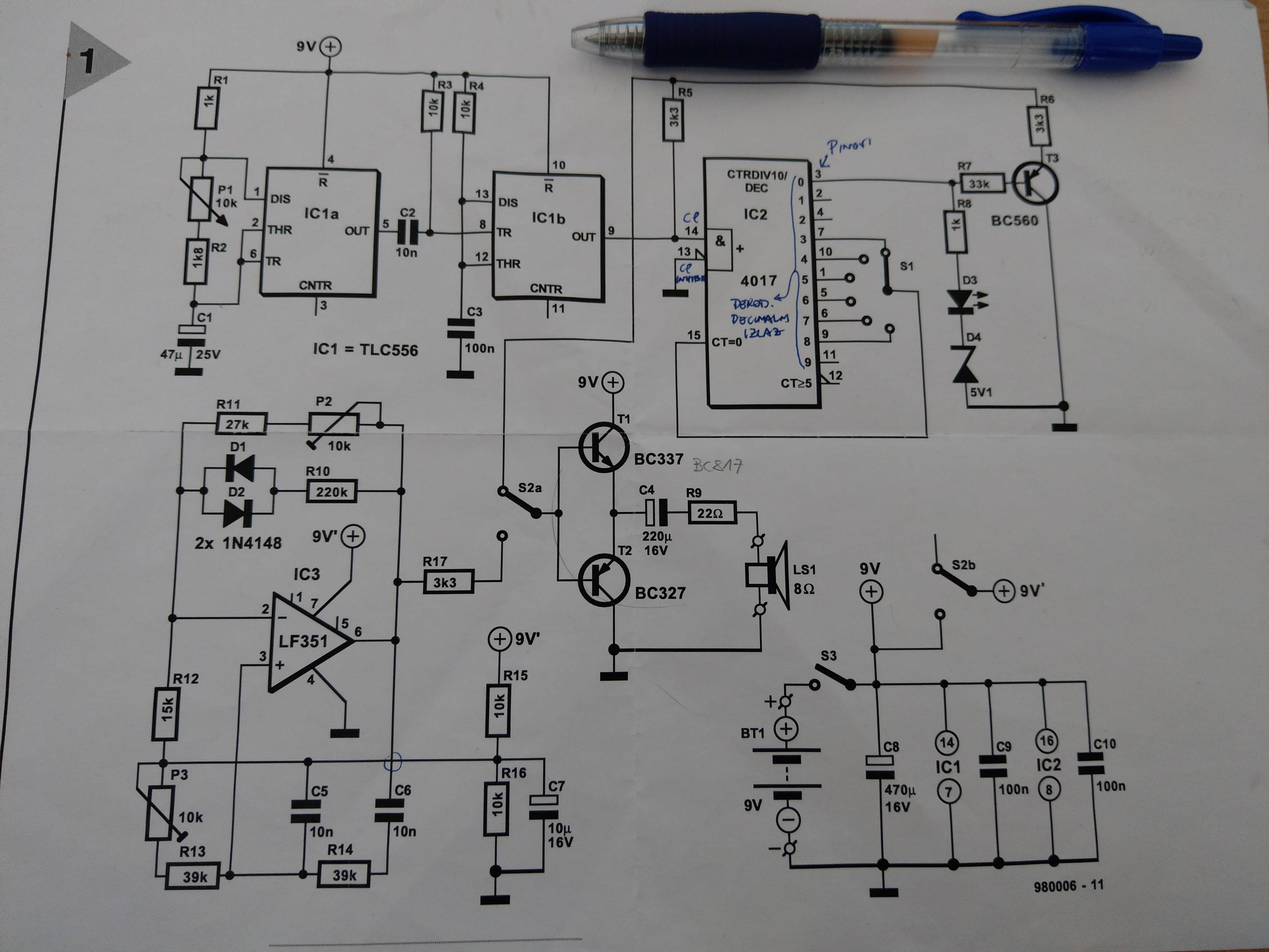
I'm having trouble understanding what the upper part of an electronic metronome depicted in the below schematic does.
I already asked about the lower op-amp part in another topic, but I also can't figure out how the upper part works.
This is my understanding of what the upper part does:
The TLC556 component is basically 2 TLC555s in 1 package. The first 555, marked as IC1a, is wired as an astable and generates a square wave at its output. The frequency and duty cycle of the square wave can be set by changing the value of the variable resistor marked as P1 on the schematic. Using the formulas from the datasheet, the duration of the high logic level can be calculated as C1*(R1+P1+R2)*ln(2) and the duration of low logic as C1*(P1+R2)*ln(2).
By setting the resistance of the variable resistor P1 to 0 Ohm, the output square wave frequency is 6.673 Hz with a duty cycle 60.9:39.1, and setting the resistance of P1 to 10 kOhm output frequency is 1.2478 Hz with 52:48 duty cycle.
What I can't seem to figure out is what does the other 555, marked as IC1b, do? I believe it's wired as a monostable, which means that, when the output of the first 555 goes low, the second 555 gets triggered and its output goes logic high. The duration of logic high is set by R4 and C3 and can be calculated by 1.1*R4*C3, according to the datasheet. That would mean that the logic high pulse duration on the output of the second 555 is 1.1 ms, which is far less than the duration of low logic level on the first 555's output.
While the first 555's output is low, the second 555 always gets triggered (?), which means that it either gives constant high logic level at its output, or it is a square wave with a very high duty cycle. So I'm wondering what exactly is the point of the second 555?
The output of the second 555 is connected to the clock input (pin 14) of a 4017 decade counter, and by selecting the desired output on the switch S1, we can basically set the frequency divider of the square wave on the 4017's clock input.

