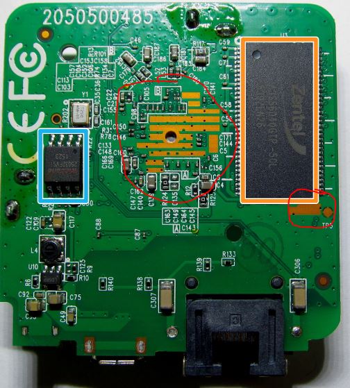
I found the following board in random research. Can anyone explain the reason for etching the green mask in red color circled area and that too patterned?

The other side of etch is the processor IC.
I found the following board in random research. Can anyone explain the reason for etching the green mask in red color circled area and that too patterned?

The other side of etch is the processor IC.
As comments have already pointed out, it's being used as a heat sink. The vias in that area connect to the thermal pad on the bottom of the IC, which is in turn connected to the substrate to conduct heat from the chip itself. Since the processor is likely surrounded by its own pins, the most effective way to spread out the heat is on the ground plane on the bottom side of the board.
You can see that a large section of the side in the photograph is contiguous ground plane, and that traces have been routed around it to keep it large. It still has to go somewhere, though, and the most convenient process for that is convection or conduction. Not having the assembly, I can only guess that it's convection, but the large center hole makes me wonder if it was contacting something solid.
In either case, the solder mask serves as an insulator preventing the heat from leaving the ground plane. It's removed to allow better heat transfer.
As far as the distinctive shape of the cutout, I can only assume that the designer of that board knew more than I do, either about convection in general or about the specific requirements of that product.