3
\$\begingroup\$

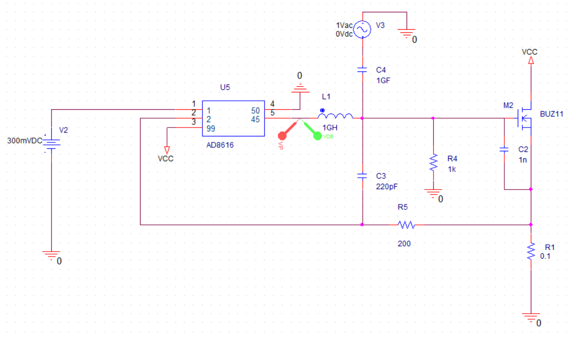
I've tried to build this opamp/mosfet current source, and been struggling to make it stable. When simulating the open-loop gain in PSpice. I've set it up like this, which should give Vout = -AB at the output of the opamp.
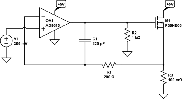
schematic

simulate this circuit – Schematic created using CircuitLab

enter image description here

And it looks to have a huge phase margin on the plot:

enter image description here

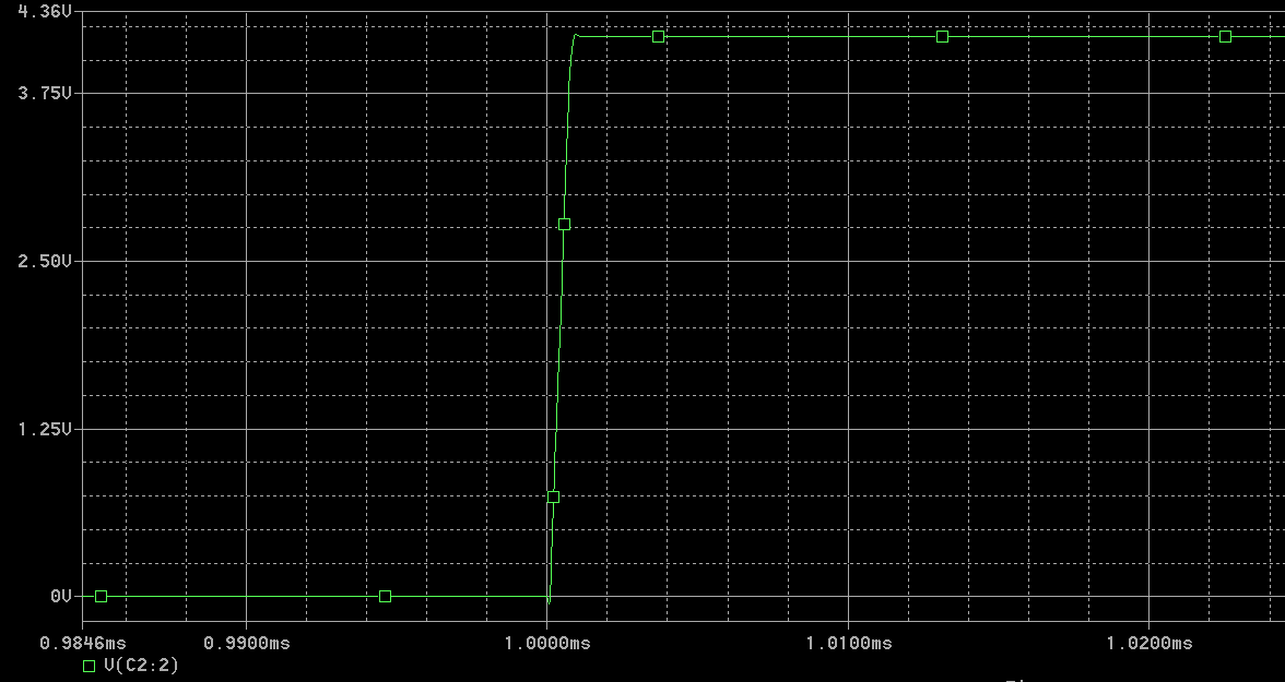
Which also shows if I step the input with a 1 ns rise pulse, that it is very stable(measured at the output of the opamp):

enter image description here

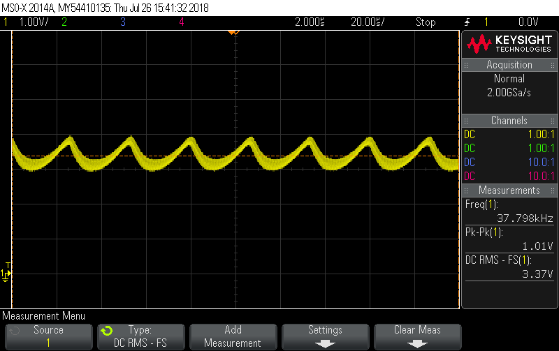
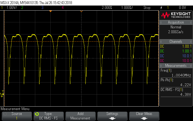
But unfortunately it is very unstable on the prototype PCB that I made. The first picture is when the input voltage is 0, or below 10 mV. The second picture is when I increase the voltage to around 70 mV at the input:

low input voltage (<10 mV)

Higher input voltage(around 70 mV)

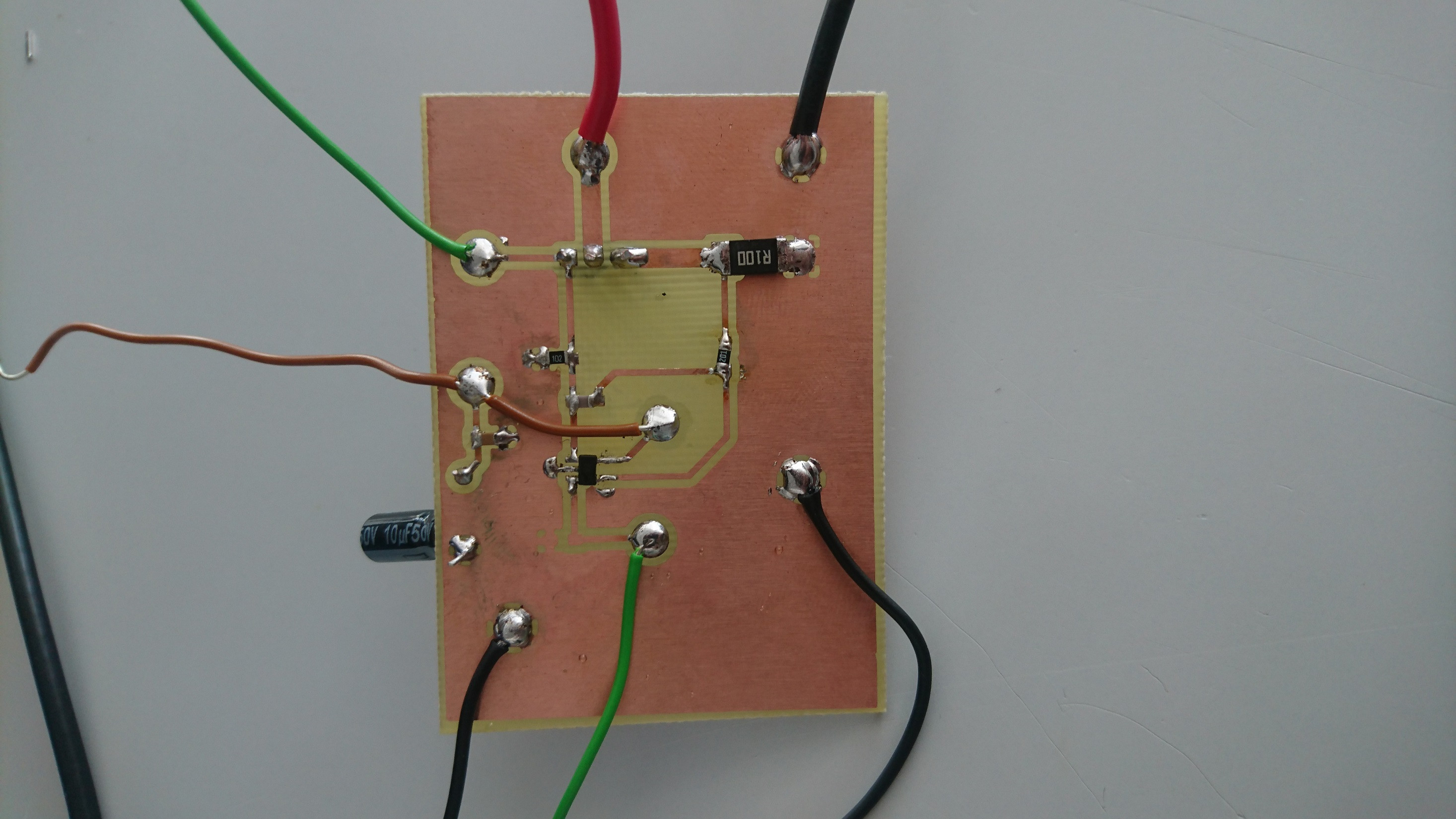
Here is a picture of the PCB:

enter image description here

I could not route the 5 V for the opamp on the single sided PCB, so I made a small jumper. At the input of the 5 V there is a 10 µF electrolytic and a 100 nF ceramic as a bypass.

The green wire at the bottom is the input to the opamp. The other green wire is measurement at the gate of the opamp.

How can I simulate this circuit correctly?

How can I stop the oscillations in my circuit?

EDIT: I forgot to mention that I added C2 because the mosfet I'm using (ST P36NE06) has more input capacitance than this BUZ11 FET has.

\$\endgroup\$
10
  • \$\begingroup\$ Your op amp is U5 - an AD8616? Your schematic doesn't seem to agree with online docs for that device. \$\endgroup\$
    – mike65535
    Commented Jul 26, 2018 at 19:27
  • 2
    \$\begingroup\$ My suspicion is that you have too much impedance on your 5V input line. Can you try adding an additional decoupling capacitor as close to the chip's power input as possible? \$\endgroup\$
    – Jules
    Commented Jul 26, 2018 at 19:28
  • 1
    \$\begingroup\$ You ask about a opamp, but don't show one in your schematic. Closing as unclear. \$\endgroup\$ Commented Jul 26, 2018 at 19:43
  • \$\begingroup\$ What is C2 for? You are driving a capacitive load. Try to isolate it with a series resistor of a few 100's ohms. Also try to solder a decoupling capacitor on the Vdd/Vss pins. A through hole ceramic will do if you can't solder an smd one. \$\endgroup\$
    – Mike
    Commented Jul 26, 2018 at 19:48
  • 1
    \$\begingroup\$ @OlinLathrop: U5 is an opamp. It doesnt have the right symbol, because its just ported directly from a model from AD's site. \$\endgroup\$
    – Linkyyy
    Commented Jul 26, 2018 at 20:38

2 Answers 2

6
\$\begingroup\$

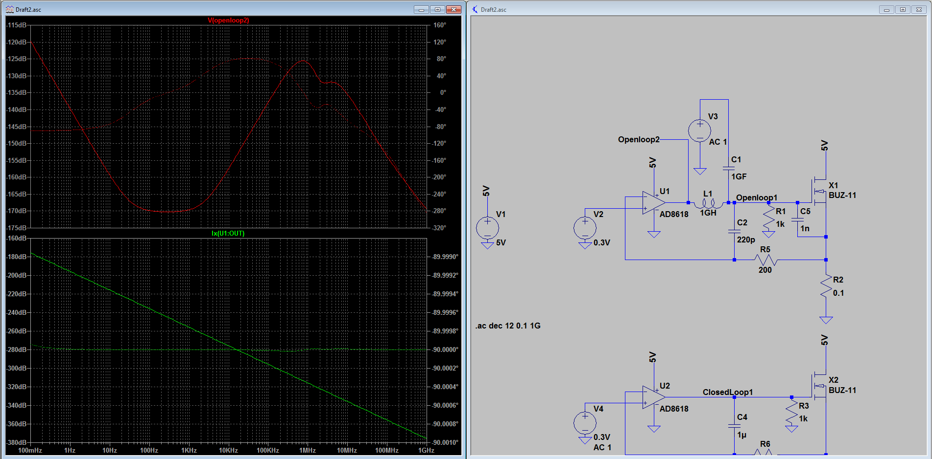
The problem is the loop has not been compensated correctly, it wants to oscillate as shown your graph on the red scope trace (the voltage probe) I have a similar plot below:

enter image description here

This can also be seen in the closed loop gain (green trace) the hill at 10Mhz indicates that there is a Q point that wants to ring around 10Mhz (but why not 1Mhz like the design resonates at? stay tuned).

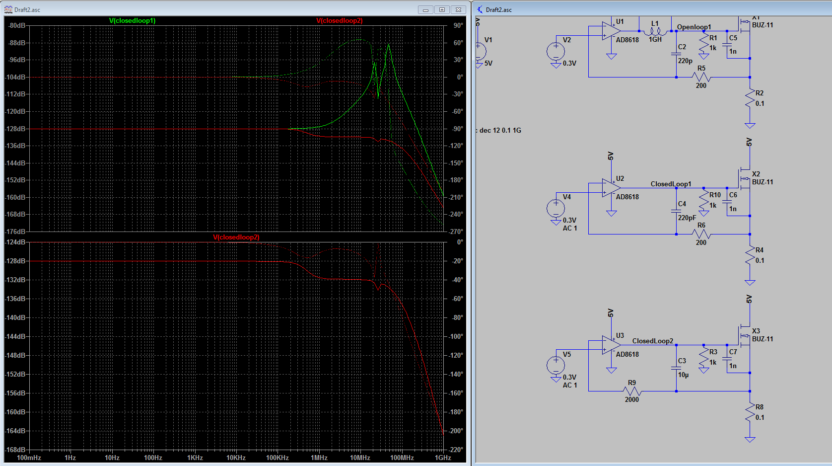
So how to fix this? Use a lot more capacitance, 10uF and move it to the other side of the resistor. After doing so you get the red trace, which shows very little ringing.

enter image description here

There are a few other caveats, there has been no parasitics simulated! So either build your design as close as possible to the schematic OR simulate the parasitics by estimating them from the board. Part of the reason for the simulation showing a resonance point at 10Mhz and the design at 1Mhz is parasitic inductance has not been simulated.

Cables will contribute 10nH's, the traces can also have some inductance and resistance. I could go into much detail but have ran out of time. The way to calculate this is with trace inductance/resistance calculators.

In these kind of circuits inductance can change things, where it normally can be neglected. You may also want to include the source resistance of the wire and the simulation as the current source and the power filter caps can also contribute to resonance.

\$\endgroup\$
8
  • \$\begingroup\$ Thanks for your answer! I dont quite understand why it helps to move the capacitor to the other side of the resistor. Now it is basically just in parallel with Cgs of the MOSFET, which would make it even more unstable if you ask me? Yes you are right about the parasitics, but i did not think it would have that huge of an impact in this design \$\endgroup\$
    – Linkyyy
    Commented Jul 27, 2018 at 14:33
  • \$\begingroup\$ I usually do a lot of current sources with BJT's, I'd test them with no wiring and they'd work fine, then oscillate when I plugged wires into them. After a while I learned how to simulate the wiring parasitics to compensate the wires and the loop. These circuits are counter intuitive because of the capacitance, but you need more not less. \$\endgroup\$
    – Voltage Spike
    Commented Jul 27, 2018 at 15:17
  • \$\begingroup\$ If you like the answer upvote and mark the appropriate answer as answered meta.stackexchange.com/questions/126180/… \$\endgroup\$
    – Voltage Spike
    Commented Jul 27, 2018 at 15:18
  • \$\begingroup\$ Oh, and I just saw Andy's answer about the capacitance, it may be possible to insert a pole at 100khz without a 1uf capacitor, otherwise change the op amp \$\endgroup\$
    – Voltage Spike
    Commented Jul 27, 2018 at 16:31
  • \$\begingroup\$ Im not sure i follow the pictures from the simulation you made. In the openloop2 plot it looks like the gain starts rising with 40dB at 1 kHz. Why does it do that? It looks odd. \$\endgroup\$
    – Linkyyy
    Commented Jul 27, 2018 at 18:31
3
\$\begingroup\$

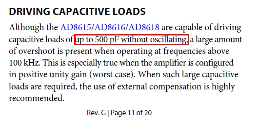
The main problem that I see is that your open loop simulation isolates the op-amp output from the gate-source capacitance with a 1 giga henry inductor. This naturally does the job of maintaining DC conditions around the loop but, and very importantly, fails to take into account how susceptible the AD8616 is to capacitive loads on the output.

For instance, if you look at figure 17 in the data sheet you can see that you are going to get "indecent" levels of overshoot with 1nF + gate-source capacitance (1.5 nF). Added to this is figure 14 and this tells you how the output impedance of the op-amp varies with frequency for certain gain levels. Your op-amp gain is practically as high as it gets (no local feedback) so you can assume the output resistance will be about 30 ohms or maybe mush more in the frequencies of interest.

Again, in your sim, this impedance is buffered by the 1 giga henry inductor and this means that your sim will not take this into account.

Circa 60 ohms output resistance and 2.5 nF has a 3dB point of about 1 MHz and adds a whopping 45 degrees to the open-loop phase shift. Note also these words in the data sheet: -

enter image description here

That is probably the last nail in the coffin.

\$\endgroup\$
3
  • \$\begingroup\$ Thanks for your answer. Yes i was aware that this opamp is not supposed to drive more than 500pF, that is why i am trying to compensate it to make it stable :) I see what you mean about the isolation of the mosfet from the gate. But from a control design point of view, the loop gain should not be different? And as long as the DC bias is still intact, shouldn't this be alright then? \$\endgroup\$
    – Linkyyy
    Commented Jul 27, 2018 at 14:39
  • \$\begingroup\$ Could you recommend another way of measuring the loop gain then?`:) \$\endgroup\$
    – Linkyyy
    Commented Jul 27, 2018 at 14:41
  • \$\begingroup\$ You could drive it like you are doing but add an extra MOSFET's worth of capacitance directly at the output of the op-amp but clearly, that will cause oscillation as per the snippet from the data sheet. \$\endgroup\$
    – Andy aka
    Commented Jul 27, 2018 at 14:44

Your Answer

By clicking “Post Your Answer”, you agree to our terms of service and acknowledge you have read our privacy policy.

Not the answer you're looking for? Browse other questions tagged or ask your own question.