0
\$\begingroup\$

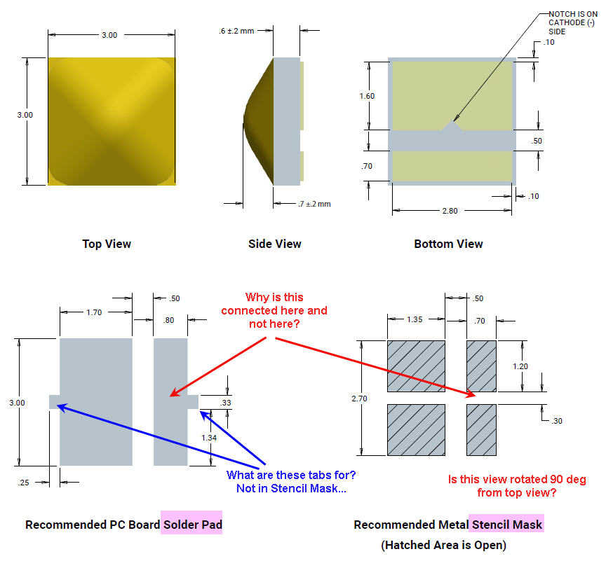
I am using Autodesk Eagle. Need to create a footprint for CREE LED XHBAWT which is in the XLAMP XH-B series. I do not understand the Datasheet drawing of the footprint, attached.

  1. Are the lower views rotated 90 deg from the upper views? If so that seems odd.
  2. Why is there the horizontal gap on the stencil mask on the right, but not on the solder pad on the left?
  3. What are the little "tabs" on the Solder pad drawing?
  4. Do I need the Solder Pad drawing? Don't I just use the Stencil Mask Drawing for my pads?

Data Sheet page 9

\$\endgroup\$

1 Answer 1

4
\$\begingroup\$
  1. Yes they are rotated.

  2. The "Stencil Mask" is a physical metal stencil created to be used by the assembly house to print solder paste. The grid reduces the solder coverage to the typical 70% or so for a pad. For example the tab on TO252 package usually is split into 4 or 9 . Also the polarity notch means that a bit less solder is required in that area. If you have too much solder coverage it might short under the device.

TO-252:
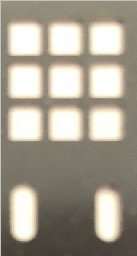
enter image description here

  1. Not sure why they put the tabs on there, but they are dimensioned so they probably belong. They may be intended to draw out excess solder to prevent shorting.

  2. The pads represent the copper, the stencil mask defines the holes where the solder paste is printed. They're on different layers in your footprint, and both are necessary (unless you're planning on never making a stencil and always hand soldering). Note that the copper dimensions are larger than the solder paste.

Note: They don't define the solder mask layer, but you should. In particular, the 'tabs' should probably be free of solder mask (as well as the pads proper, of course).

Typical stencil:
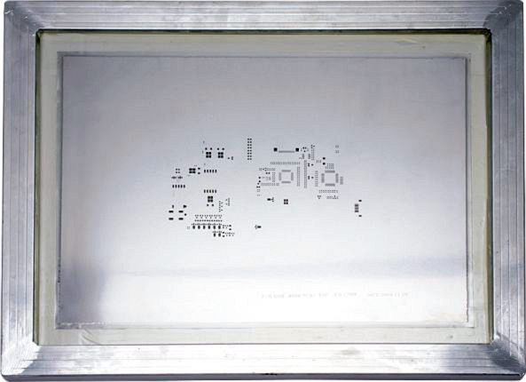
enter image description here

\$\endgroup\$
2
  • 1
    \$\begingroup\$ Too much solder under a large pad can also "float" the part above the plane of the board and prevent wetting of smaller pins (which then end up not connected). \$\endgroup\$ Commented Aug 20, 2018 at 4:03
  • \$\begingroup\$ Thanks Spehro and Dean. In Eagle I think the solder mask layer is tcream layer 31, right? \$\endgroup\$
    – BlueSky
    Commented Aug 21, 2018 at 22:57

Your Answer

By clicking “Post Your Answer”, you agree to our terms of service and acknowledge you have read our privacy policy.

Not the answer you're looking for? Browse other questions tagged or ask your own question.