1
\$\begingroup\$

(using KiCad 4.05 at the moment)

I’ve been following video and blog instructions on how to create a PCB.

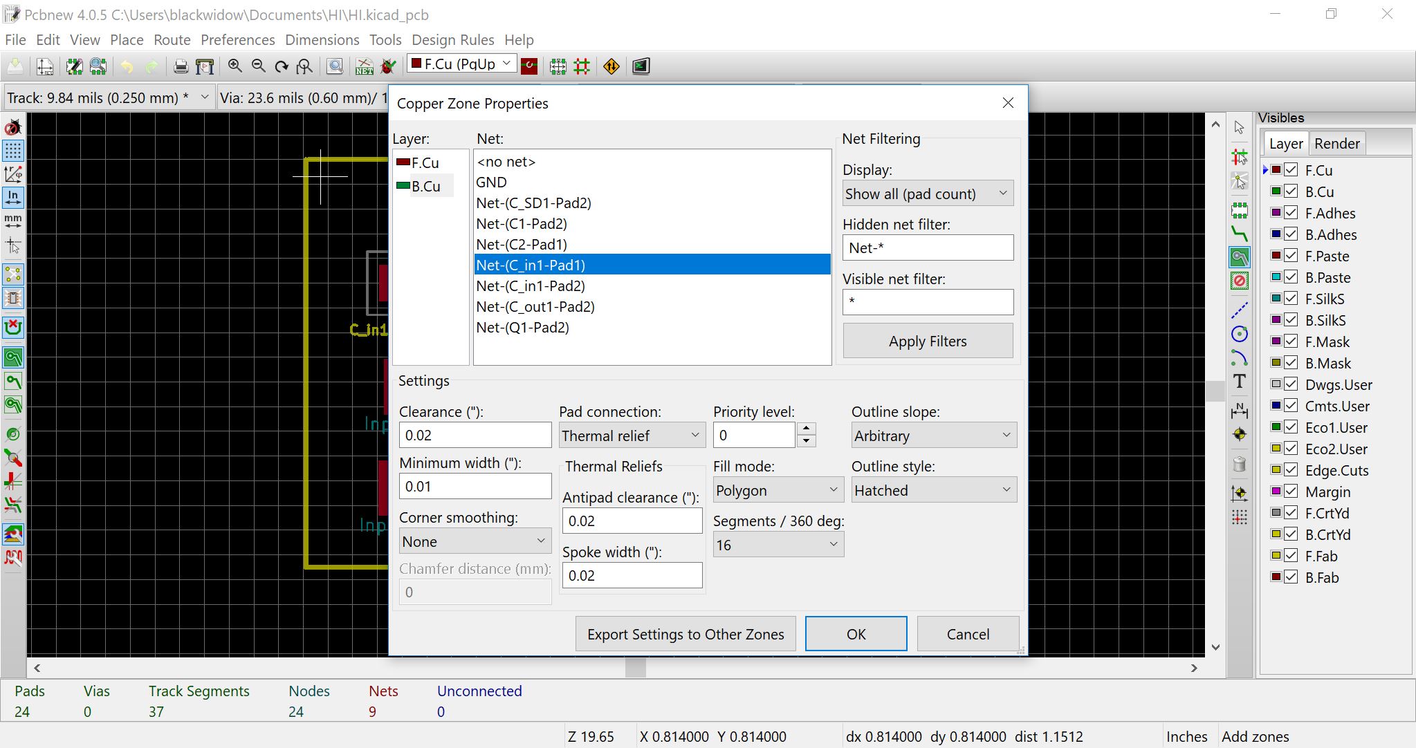
Everything has been straightforward (have used EAGLE a bit many years ago) up until ‘add filled zones.’

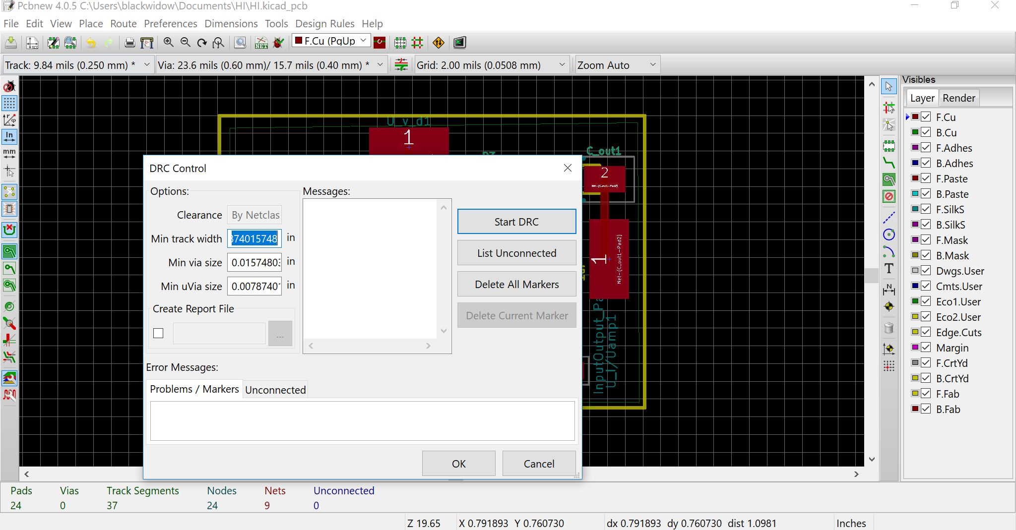
I’ve also performed ‘DRC control,’ to no avail.

It seems when i select ‘no net,’ it does color the bounded area.

Help would be much appreciated. Thanks

(unlike what’s selected in the image, I chose GND, if it is relevant)enter image description here
enter image description here

enter image description here

\$\endgroup\$
1

2 Answers 2

4
\$\begingroup\$

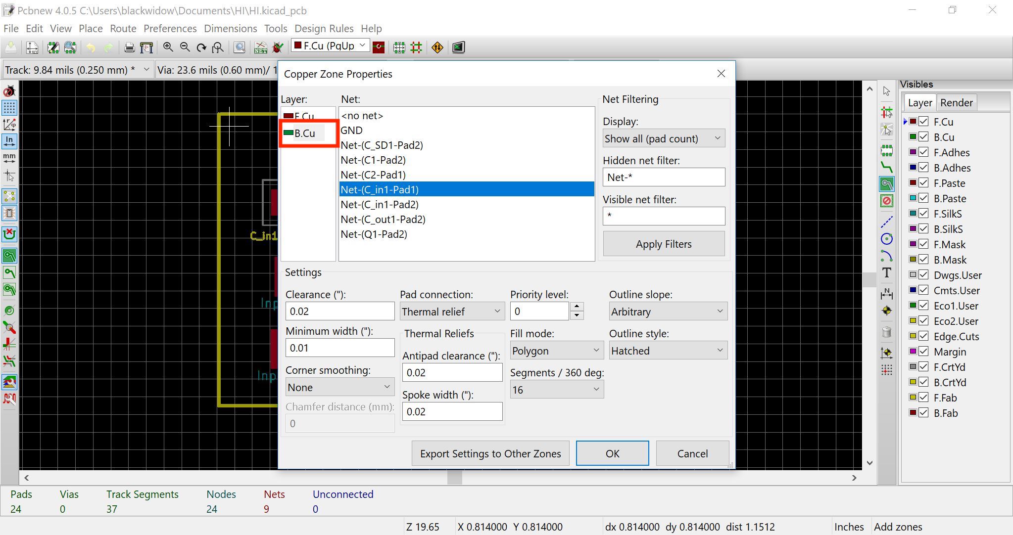
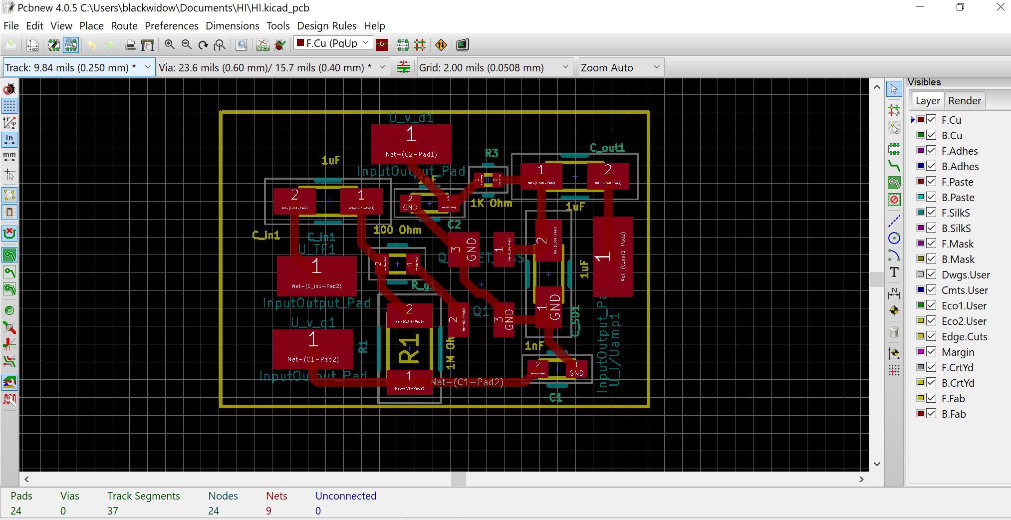
It looks like all of your components are SMD, so they only exist on one layer (F.Cu) and you are making your zone on the backside (B.Cu). If you move the zone to the front layer, it should work. You can also place a via to bring the signal from your pad in the front layer to the back.

enter image description here

\$\endgroup\$
3
\$\begingroup\$

KiCad only fills zones if they are connected to a pad in one way or another. This can happen by using a trace, a via or the zone is in direct contact with the pad. As @seth already mentioned you can use vias to get GND to the back side of your PCB.

A GND zone on the Back only makes sense if you really use it for connecting something. (In most cases you want an uninterrupted zone for EMC reasons. And you want your GND connections to be very short.)


Over at the forum a user made some tests about what the requirements are to get kicad to fill a zone: https://forum.kicad.info/t/filled-copper-zones-not-showing-up-in-gerbers-printouts-3d-view/8401/9

\$\endgroup\$

Your Answer

By clicking “Post Your Answer”, you agree to our terms of service and acknowledge you have read our privacy policy.

Not the answer you're looking for? Browse other questions tagged or ask your own question.