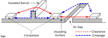
How to measure creepage distance over pcb ? Is creepage and clearance distance measure by pbc layout or soldering?
-
\$\begingroup\$ If your soldering does not closely follow your PCB layout, you're probably doing something wrong. \$\endgroup\$– Dave TweedCommented Sep 30, 2018 at 14:56
-
\$\begingroup\$ Pcb layout with masking are not taken into account to measuring creepage distance \$\endgroup\$– Vikas VermaCommented Sep 30, 2018 at 15:12
-
\$\begingroup\$ Is creepage distance measure from solder point or end of pcb layout with masking \$\endgroup\$– Vikas VermaCommented Sep 30, 2018 at 15:14
-
\$\begingroup\$ creepage is dielectric contamination and air is much better than surface gap read more electronics.stackexchange.com/search?q=creepage elsewhere there are safety standards for levels of contamination RH+dust + salt spray if applicable. \$\endgroup\$– D.A.S.Commented Sep 30, 2018 at 15:28
2 Answers
How to measure creepage distance over pcb ? Is creepage and clearance distance measure by pbc layout or soldering?
This might help: -
Picture from this site.
-
\$\begingroup\$ But how to measure creepage distance between primary pin to secondary pin of transform at pcb when any another conductive surface or component comes on the way of creepage distance \$\endgroup\$ Commented Sep 30, 2018 at 15:05
-
1\$\begingroup\$ If the "thing" coming in the way cannot be relied upon for its insulation properties then it should be regarded as a conductor. If it can be *somewhat" regarded as an insulator under normal conditions then you might be able to regard it as equivalent to air, else regard it as a conductor. Safety first. \$\endgroup\$– Andy akaCommented Sep 30, 2018 at 15:11
-
\$\begingroup\$ If conductor is on way of creepage distance and how to measure?? Is measured first A point to conductor then skip creepage distance of conductor then to the final B point as regards A +B distance for creepage \$\endgroup\$ Commented Sep 30, 2018 at 15:25
-
\$\begingroup\$ The width of the conductor would be regarded as zero unless it was a suitable earth conductor then it would negate the need to determine the full creapage path. But otherwise, skip the conductor width. \$\endgroup\$– Andy akaCommented Sep 30, 2018 at 15:44
-
\$\begingroup\$ You mean yo say just add point A to conductor and skip conductor width and B from second end point as A+B distance without conductor width. \$\endgroup\$ Commented Sep 30, 2018 at 15:55
Creepage occurs from excited ion flow in an insulator between charges and conductors with a voltage potential difference. Excess solder flux may be an issue if excessive in the gap but that would be abnormal. Imagine it as a sticky collector of dust. This is why boards are kept clean and dry with suitable air gaps where needed when AC grid potential power is behind these voltages.
Other relevant info, to put things into perspective.
Partial Discharges could be like the dust in the air with vast distances in km from cloud to earth or nm in semiconductor lithography where contamination is limited by clean room technology yet ESD is still a threat to 12nm epitaxial gaps or the ribbed insulators in transmission towers which use HV bushings surface creepage is measured in kV/mm for the surface path length which is increased the air gaps in each ringed rib but then cleansed by rain yet also bridged by the water's capacitance.
But in this case, you are referring to PCB surface creepage. It would be measured by a HIPOT but is significantly 10%to90% (worst case) degraded by gross contamination with dust accumulated by fans and humidity. This is why an air gap is preferred. A streamer arc is followed by an arc when HIPOT fails so the tester ought to be currently limited with for example 3 to 4kVdc and 1M to 10M resistance in series with the probe to prevent capacitance discharge. E-field gradients are increased with sharp points on the conductors which lower the breakdown withstanding voltage from power surges such as inductive lightning surges.
It may be measured in giga or mega ohms but what really happens is once charge flow starts, it accelerates the resistance drops and capacitance rises until the medium has a weak link and discharges. If this bridges the entire gap then it becomes an avalanche diode like arc with all the follow-on current available. Electrical RTV Silicone is often used around high voltage triplers to reduce surface creepage for example. SParkplug wires are made of long rubber insulation for better protection from dust accumulation. Some parts are usually protected from dust to create better creepage barrier such as the housing for the inductive coils.

