Let me detail what I perceive from reading you:
- You know you want to use LEDs and you think these LEDs will require about \$3\:\text{V}\$ to operate (or more, perhaps, but probably not less.) This idea of "operation" isn't precise, since you've not provided a specific LED to consider nor how bright it must appear when operating. Etc. But at least this is a vague goal of sorts.
- You want to operate the multiplexing as "by 16" and with an effective average of \$4\:\text{mA}\$. The human eye is complex and, as it turns out, pulsing rates do have an impact on apparent sensitivity. LEDs have their own emission complexities when pulsed with currents a decade or more higher than their average, too. But assuming you have the right multiplexing rate and that we can ignore non-linear aspects of the LEDs too then a simple rule might be "good enough" for now. That is, plan to operate the LEDs at a level of at least 16X or \$16\cdot 4\:\text{mA}=64\:\text{mA}\$ peak. This will, of course, imply a still higher voltage requirement for each active LED, which is also currently unstated and unknown but at least must be recognized.
- Since this is x16 multiplexing (let's call each one of these a "row," and you have up to 32 LEDs (let's call each one of these a "column") enabled per row (fewer is okay, of course), then this means that each of the 32 column drivers (whether arranged high-side or low-side) will current-limit at just \$64\:\text{mA}\$. But each row driver on/off switch will have to support the current of up to 32 LED columns being on at the same time. That's up to \$2\:\text{A}\$ for each row switch!!!
Given the above for a moment, I think you need to plan on at least \$300\:\text{mV}\$ overhead for the BJT switch on one side. At \$2\:\text{A}\$, I might argue for still higher if this were just junk-box parts. But there are BJTs that can do it with even less, so let's stick with that number to just do a quick back-of-envelope calculation to see if we are even in the right ballpark. Since I'd like to recommend that you use a current limiter topology for each column (so that you can avoid the use of 512 LED resistors; one for each, if that was your thinking), this limiter will probably require \$1.4-1.5\:\text{V}\$ of its own. If you also figure that operating the LEDs at \$64\:\text{mA}\$ (more or less) will mean they will require something more than \$3\:\text{V}\$, then I think you can see why having a \$5\:\text{V}\$ supply rail starts to look a bit tight. However, while I think it is tight, I also think it may be achievable. So for a back-of-envelope calculation, I'd say things are somewhat tight and that there might be problems... but that if care and thought is applied and some judicious choices made, then it just might be doable and work satisfactorily for you.
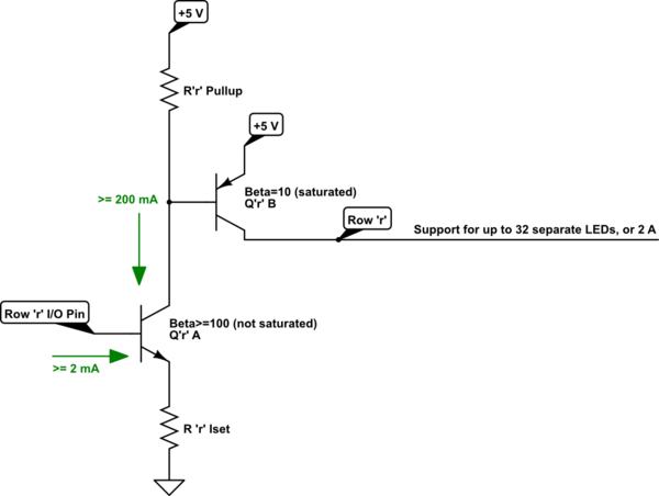
So let's take a look at a typical row switch first. In this case, I'm talking about one of the 16 rows that need to operate with a current compliance of up to \$2\:\text{A}\$:

simulate this circuit – Schematic created using CircuitLab
I've intentionally tried to keep this is uncomplicated for BJTs, as possible. To do that, I've decided to make \$Q_{r_A}\$ operate as an emitter-follower and not in saturation, which would have made the base-drive a serious problem. Operating as an emitter-follower means that we can rely upon the fuller \$\beta\$ value of the BJT and this greatly decreases the required current needed to operate it. Here, I assume that \$\beta\ge 100\$ is an acceptable assumption for \$Q_{r_A}\$.
One serious problem with the above topology is that it requires the collector of \$Q_{r_A}\$ to be above the base voltage, when activated. If everything you have is running off of a single \$5\:\text{V}\$ supply, then this isn't going to work. And I think you are clear that everything is running off of a single \$5\:\text{V}\$ supply.
If, instead, we converted \$Q_{r_A}\$ to have to act as a saturated switch rather than operating as an emitter follower, then we'd be stuck needing a base current of about \$20\:\text{mA}\$. That's not going to fly well.
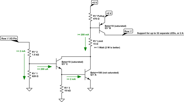
So, keeping with BJTs, one approach is to use the Darlington configuration to further reduce the I/O pin current compliance requirement. To achieve this, add yet another BJT as follows:

simulate this circuit
As you can see, it's gotten a little more complicated. But at least it should work out okay. You've written that you can't get FETs, so this would be an approach using only BJTs.
The design is as follows:
- The maximum compliance current for \$Q_{r_B}\$ is \$2\:\text{A}\$. Since it must operate as a switch, we have to assume that \$\beta\le 10\$. (Or maybe \$\beta\le 15\$, but this is just a matter of what you feel comfortable with.) This means that the base current for \$Q_{r_B}\$ is about \$200\:\text{mA}\$.
- The next question will be about dissipation for \$Q_{r_B}\$. Since the collector current is so high, this all depends on the \$V_{\text{CE}_\text{SAT}}\$. It could be anywhere from about \$50\:\text{mV}\$ for a D45H11 (big TO-220 package) to perhaps \$600\:\text{mV}\$ for some small signal BJT like a 2N3906. Basically, I think this means you will be looking for a TO-220 packaged device here. So let's go with the D45H11 in TO-220 packaging, for now.
- The base-emitter voltage for the D45H11 will be on the order of about \$800\:\text{mV}\$ (I'll bump that up a little to be safer.) Assuming that \$Q_{r_C}\$ is saturated when on, we have to figure that the collector voltage for \$Q_{r_A}\$ will be about \$1\:\text{V}\$. So from this we can compute \$R_{r_\text{LIMIT}}\approx \frac{5\:\text{V}-1\:\text{V}-850\:\text{mV}}{200\:\text{mA}}\approx 15\:\Omega\$.
- In order for the divider to be "stiff" with respect the base current required for \$Q_{r_C}\$, the divider current needs to be about \$2\:\text{mA}\$. (About 10X the required base current.) Assuming a slightly loaded I/O pin output of about \$4.8\:\text{V}\$, that \$R_{r_2}\approx \frac{4.8\:\text{V}-850\:\text{mV}-650\:\text{mV}}{2\:\text{mA}}\approx 1.5\:\text{k}\Omega\$ and \$R_{r_1}\approx \frac{850\:\text{mV}+650\:\text{mV}}{2\:\text{mA}-200\:\mu\text{A}}\approx 820\:\Omega\$.
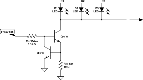
This would be the high-side row driver. Now the low-side current-limiting driver might look like the following:

simulate this circuit
In this case, you enable as many of these columns as are appropriate (up to all 32 of them) when a row is activated.
So the '595 devices support 32 column bits and are programmed with a 32-bit word before activating one of the high-side rows are activated. Then you hold the activated row for the appropriate period and turn it off, again. Re-program the '595 chain for the next 32 column bits, and then activate the next row in sequence.
Something like that, anyway.
Questions remain about using a 74LS595 (you don't state the family.) The LS family (still not uncommonly found today) is spec'd to source \$400\:\mu\text{A}\$ and perhaps sink as much as \$8\:\text{mA}\$. When sourcing, the output voltage will be perhaps \$3.6\:\text{V}\$, not the \$4.8-5\:\text{V}\$ I assumed in the above circuit. So already the value for one of the resistors I gave is wrong (I was over-driving it, though, assuming plenty of output drive current compliance of more than \$1\:\text{mA}\$.) The other part of the question is whether or not \$400\:\mu\text{A}\$ is sufficient. It may be. But \$\frac{64\:\text{mA}}{\beta\ge 100}=640\:\mu\text{A}\$ and that's perhaps a problem. If you assume the \$\beta\$ is higher than that in operation, you can probably get by.
But this will be a question for you to worry about. You might need a pull-up resistor to aid the output when HI (added current from this resistor will be sunk, when LO, but the low output can probably handle the addition if you are careful about computing the pull-up resistor value.)
A modified version of the current limit is then:

simulate this circuit
For this, I computed \$\frac{3.6\:\text{V}-1.5\:\text{V}}{400\:\mu\text{A}}\approx 5.6\:\text{k}\Omega\$.
In summary, I think your situation is a bit tight but that it may be workable.
The D45H11 (or its complement the D44H11, if you reverse the high-side vs low-side arrangements) will present fairly low \$V_{\text{CE}_\text{SAT}}\$ when operated as a switch (perhaps \$100\:\text{mV}\$ or even slightly less) and can easily handle the required current compliance and dissipation (which will be fairly low and probably barely above ambient to the touch.) You can certainly select something else, but it is almost certainly not going to be a small signal device (not anything packaged in a TO-92.) Because of the compliance currents required, the base drive circuit is more complex, resulting in the use of a total of three BJTs. Also, the \$15\:\Omega\$ resistor will need to support at least \$1\:\text{W}\$, which is big already, and might be better spec'd at twice that or \$2\:\text{W}\$ just to be absolutely safe. So this part of the circuitry will have at least two large parts in it. (On the somewhat lucky side, you only have 16 of these and that's better than if it were 32, instead.)
The current regulation circuit will require about \$1.5-1.6\:\text{V}\$ of overhead, as well. Because the collector current and \$V_{\text{CE}_\text{SAT}}\$ will be low enough for a small signal device packaged in TO-92, you can use smaller BJT devices here. Also, none of the resistors dissipate much, so they can also be small.
By doing active current limiting on each column, rather than using a resistor for each LED, you use 32 current-limiting circuits instead of 32 switch circuits plus 16 times 32, or 512, resistors. I consider the current-limit circuits to be only slightly more complex and worth it in order to save all those resistors.
Taken together, I think you can expect to see as much as about \$1.6-1.7\:\text{V}\$ drop in the circuitry surrounding any particular LED, leaving up to \$3.4-3.5\:\text{V}\$ for the LED itself. This just might cut it for you. But without the LED specs, it is hard to know for sure. But at least you have an idea what to look for in your LED when operating at about \$65\:\text{mA}\$.
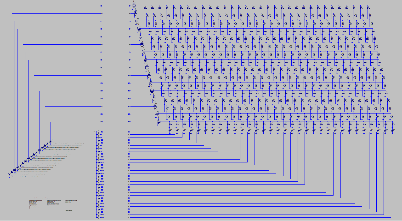
I just tried a full 512 LED test in LTSpice, with multiplexing behavior included (I can provide the netlist, if needed, but it is long.) Seems to work as given above. So I'm happy now.

(In the above diagram I've used convenient (existing) symbols from the LTSpice library rather than developing custom diagrams. This means you might see a "tetrode vaccum tube" symbol on the schematic, for example. But the only reason is that it was convenient. I wrote short SUBCKT "subroutines" for those that replicate the BJT circuit. So it is still a BJT circuit even if the image appears a little odd.)
