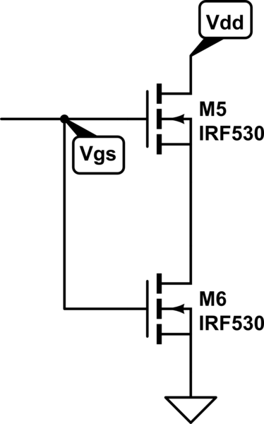
When two N-channel MOSFETS are connected in series, with common gate connections, then how can I analyze this circuit to determine Id through these MOSFETS, as a function of Vgs and Vds?

simulate this circuit – Schematic created using CircuitLab
When two N-channel MOSFETS are connected in series, with common gate connections, then how can I analyze this circuit to determine Id through these MOSFETS, as a function of Vgs and Vds?

simulate this circuit – Schematic created using CircuitLab
\$V_{gs}(M5) = V_{gs}(M6)-V_{ds}(M6)\$
If \$M6\$ is in saturation, \$V_{ds}(M6) > V_{gs}(M6)\$.
So what mode are \$M6\$ and \$M5\$ in?
This is a question that looks quite simple, but is actually very difficult.
Different voltage combinations of Vgs and VDD will cause NMOS to operate in different modes, and even the weak inversion mode needs to be considered (occurring when Vgs is slightly larger than Vth).
In order to answer this question, I do not use the formula in the textbook for calculating ids, but choose the EKV model I introduced in this answer. The EKV mode can be used in all operating areas of MOSFETs, so it is very suitable for this problem.
First, let me change your schematic slightly and add the symbol Vx, which is the voltage at the upper and lower NMOS connections.
In the EKV model, NMOS is regarded as a four-terminal device, VB is connected to ground, VG, VD and VS are the potential differences relative to VB respectively.
Then, for M1, the ids current equation according to the EKV model is as follows.
Similarly, for M2, the ids current equation according to the EKV model is as follows.
Next, since these two NMOS are connected in series, it is obvious that ids1=ids2. After simplifying the formula in Mathematica, we can get
If written as a latex formula, it is
$$\log \left(e^{-\frac{n (\text{Vdd}+\text{Vx})-\text{VG}+\text{VTO}+\text{Vx}}{2 n \text{UT}}}+1\right)-\log \left(e^{-\frac{n \text{Vx}-\text{VG}+\text{VTO}}{2 n \text{UT}}}+1\right)-\log \left(e^{-\frac{n \text{Vx}-\text{VG}+\text{VTO}+\text{Vx}}{2 n \text{UT}}}+1\right)+\log \left(e^{\frac{\text{VG}-\text{VTO}}{2 n \text{UT}}}+1\right)=0$$
Obviously, this is a rather complex formula, so the problem is much more difficult than we expected.
OK, let's verify it in LTSPICE.
According to the model parameters of LTSPICE, for IFR530, VTO=4V. In addition, LTSPICE has default values of n=1 and UT=26mV.
(1) When VG = 5V, Vdd = 5V, in theory we get Vx = 0.333V
in simulation we get Vx = 0.331V
(2) When VG = 8V, Vdd = 5V, in theory we get Vx = 1.333V
in simulation we get Vx = 1.573V
Note that I do not consider the influence of lambda in the theory, so there will be a certain deviation from the simulation. But I think this gives enough insight for a circuit designer.
Finally, I show a figure of Vx vs Vdd. It can be clearly seen that Vx will go through different stages when Vdd changes. So this is actually a pretty interesting and also complicated problem.