0
\$\begingroup\$

I recently ordered three proto PCBs from a small PCB company. This board house produces Gerber files in-house from their proprietary PCB layout files, and provides this Gerber set to the user on delivery of the PCBs... or so I thought. In the Gerber file set I received the paste mask layers (.GTP and .GBP) are missing from the set. I now suspect that they do that on purpose as they also sell paste stencils. But that is another matter.

Since I have access to Altium Designer 17 down the hall, I decided to rename the gerber file extensions to those used by Altium, and import these 8 files into CAMTASTIC. The import went fine with no problems, and viewing them looks as if these layers are just fine. Now my question...

Can CAMTASTIC generate the missing paste masks (.GTP and .GBP) from the information contained in just these imported files? It seems like there may be enough information to do this, however I'm not that familiar with CAMTASTIC to figure out how to do this. (I'm borrowing evening time on this Altium machine.) The file sets are listed in the attachment.

enter image description here

\$\endgroup\$
7
  • \$\begingroup\$ The GTP and GBP names are by no means universal, they're just the names Altium uses. Other tools use completely different names. Are you sure the stencil data isn't there under some other name? \$\endgroup\$
    – The Photon
    Commented Nov 16, 2018 at 23:49
  • \$\begingroup\$ Each of these files has a comment on the first few lines such as * G4 Top copper layer * so I have checked all of those. The number of Gerber files in the file they sent is only 8 so it's pretty obvious that this is a stripped down set. \$\endgroup\$
    – Doug12745
    Commented Nov 17, 2018 at 0:41
  • \$\begingroup\$ The manufacturer included this comment with the Gerber folder. They list the GTP and GBP layers but are missing from the set. Each file can be identify by its extension: .SLK = top silkscreen layer .SMT = top solder mask layer .TOP = top copper layer .GTP = top paste layer .INT = top inner copper layer .BOT = bottom copper layer .INB = bottom inner copper layer .SMB = bottom solder mask layer .GBP = bottom paste layer .DRI = drill file .OLN = board outline \$\endgroup\$
    – Doug12745
    Commented Nov 17, 2018 at 0:50
  • 1
    \$\begingroup\$ Did you just ask them to provide the missing files? \$\endgroup\$
    – The Photon
    Commented Nov 17, 2018 at 0:52
  • \$\begingroup\$ Yes, by email a few days ago. They want to sell paste masks for the boards they produce at $125/mask. The PCBs only cost $100 for three. We usually do our own masks on our laser cutter. \$\endgroup\$
    – Doug12745
    Commented Nov 17, 2018 at 1:22

4 Answers 4

1
\$\begingroup\$

With the appropriate (eg soldermask file) go to the Tables/Apertures, where you should be able to change the aperture dimensions as necessary.

Do this on a copy of the original of course.

You can also do this in the final gerber file as well, the standard is available at the www.ucamco.com (the_gerber_file_format_specification.pdf)

The hitch is that if there are paste mask patterns that are not simply smaller versions of pads you may have to create some new ones and fit them in by hand (often these are thermal pads, etc.)

You should then double check the resulting gerber file either with camtastic or with GCPrevue or some other such program that can stack the soldermask and past mask layers in different colors so you can inspect visually.

\$\endgroup\$
1
\$\begingroup\$

You can generate paste masks from the solder masks quite easily, but it may be more challenging to create good paste masks without a good deal of manual effort. The information that is embodied in a good paste mask layout is simply not present in the other board fabrication layers.

If your parts are all SMD, such that every mask opening is a pad that needs paste, then you can simply use the mask layers as your paste layers. Ideally you would shrink the apertures a bit to avoid dispensing too much solder on each pad, but this method will get you fairly close with minimal effort.

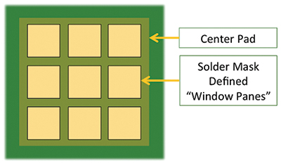
If you have parts with large pads (DPAKs, or QFN/QFPs with thermal pads), using the mask openings directly as the paste openings will not work well. You'll wind up with way too much solder and are liable to have poor leveling and even voids. Large pads should be "window paned" with un-pasted areas to control the solder volume and allow for better outgassing of the joint.

From here:

enter image description here

Lastly, and most obviously, if you have an openings that are not meant to receive paste, such as through-holes or test pads or un-tented vias, then these openings will need to be cropped out.

Your best bet, if you have the original design files for the board, is to simply create the paste layout yourself using the appropriate settings. The major benefit of doing it this way is that you only have to define all of the paste openings once in the footprint libraries, and you can easily generate paste layouts for any future boards in (depending on the CAD tool) just a few simple steps.

\$\endgroup\$
1
  • \$\begingroup\$ Excellent description and insites as to pastemasks. Thanks. \$\endgroup\$
    – Doug12745
    Commented Nov 19, 2018 at 18:10
1
\$\begingroup\$

Not completely automatically.

What you probably want to do is take the solder mask layer and use that file to generate the stencil. It may not be perfect and you'll have paste in places where you don't want it to be (e.g. fiducials, through-hole footprints, ..) but you can either ignore that (wouldn't want to do that) or delete those from within CAMtastic. Usually the paste mask pads are a little smaller than the soldermask but you might get away with it.

All in all I don't think it's worth the hassle and you should order the files from the fabricator.

Yet, I need to say this: If you make a business do work for you, always make sure that you get all the source files - ALL of them. Now they will be able to pull money from you with every little thing you want. If the business doesn't provide that option, choose another one - there are plenty. I find that approach very .. problematic.

\$\endgroup\$
0
\$\begingroup\$

Thanks all for the info. In summary, the answer is: Yes you can generate a missing paste mask from a copy of the solder mask by slightly narrowing the apertures. Some editing may be needed particularly if SMD and thru-holes are both used.

\$\endgroup\$

Your Answer

By clicking “Post Your Answer”, you agree to our terms of service and acknowledge you have read our privacy policy.

Not the answer you're looking for? Browse other questions tagged or ask your own question.