2
\$\begingroup\$

Background

The task is to add an electronic means to limit the power applied to an electric motor in an industrial setting. The operator normally controls the motor power through a lever that is mated to a 5KΩ pot:
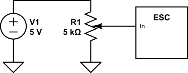
schematic

simulate this circuit – Schematic created using CircuitLab

The electronic device I want to add should be able to cap the signal to a limit, so that the signal fed to the ESC follows the relation

$$V_{\text{out}} = \text{min}(V_{\text{in}}, V_{\text{limit}})$$

or (thanks to @GlennW9IQ for suggesting it!)

$$V_{\text{out}} = V_{\text{in}} * V_{\text{limit}}$$

(in the second case, assume Vlimit is 0..1, i.e. just a normalized multiplier).

One very important detail is that whatever I add should not be able to generate a phantom signal, i.e. Vout MUST be always less or equal to Vin, even in the event of software bugs and reasonable hardware failures. To this end, I initially drafted something like this:

Draft 1

schematic

simulate this circuit

There are also other details, e.g. a relay to bypass the whole circuit if my device is unpowered. The purpose of OA1 is to buffer the input signal so it can be read through a MCU ADC pin. With this schematic, I can be reasonably sure I cannot inject a positive voltage on ESC's input, since I can only pull the pot's signal down. The problem is that OA2 cannot bring the signal to 0V if the limit signal says so, because the output will always be at least the Vf of the diode. In theory that can be fixed if I add a negative rail to V- of OA2. But in practice this is unfeasible.

Draft 2

So I have this new draft, shown here just the part to the right of OA2:

schematic

simulate this circuit

Problem

The schematic in Draft 2 is capable of pulling the pot readout hard to 0V, but I fear the feedback loop is too complicated, too high gain, and the output is going to oscillate a lot.

I've intentionally left the ?? box, because I think that's where some oscillation/stabilization components should be added (e.g. 220k||1µF to ground). The good news is that the input is fairly low-bandwidth, say 10 Hz (how fast can you turn a pot?) and it's okay if the output has some defects/overshoots, since the motor has a lot of inertia. I just don't want it to oscillate all the time.

Problem

So: how to stabilize this feedback loop and prevent any oscillations?

EDIT

Based on suggestions in comments, I've updated Draft 2 to include an integrator around OA2:
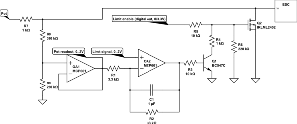
schematic

simulate this circuit

If I'm understanding the theory correctly, OA2's feedback loop is now bandwidth-limited to around 50 Hz, with -3dB corner frequency around 5Hz. Will these additions suffice?

EDIT #2

As suggested by @GlennW9IQ, I presented the option that the limit value modulates the input, i.e. you can still use the full range of the pot, however your output range is rescaled according to the limit. See the updated formulas for Vout.

EDIT #3

Additional circuit/system details:

  • My device has a 3.3V power rail, hence the need for resistive dividers, opamp buffers, etc.
  • I don't have a 5V rail handy (I don't want to use the one from the ESC-to-pot cable).
  • The Vlimit signal is generated by a 8-bit DAC and its Vref can be either 3.3V or 2.048V.
\$\endgroup\$
18
  • \$\begingroup\$ I would (for a first cut) make the second amplifier an integrator to roll off the gain at higher frequencies. Probably add a fairly high value parallel resistor across the cap for the feedback loop. \$\endgroup\$ Commented Dec 2, 2018 at 15:25
  • \$\begingroup\$ 1: your op-amp is hooked up as a comparator, it'll never give you the smooth limit you seek. Google "minimum of two voltages circuit" or some such. \$\endgroup\$
    – TimWescott
    Commented Dec 2, 2018 at 16:17
  • \$\begingroup\$ 2: Once you figure out the voltage you want applied to the ESC, you can use a FET (or BJT), as the final amplifier element, but you want the inner loop of the op-amp to be an integrator. Google "op-amp constant current sink" for guidance (I hope that works!). \$\endgroup\$
    – TimWescott
    Commented Dec 2, 2018 at 16:19
  • \$\begingroup\$ Hmm, just to be sure: the capacitor (and parallel resistor) is across the output and inverting input of OA2? \$\endgroup\$
    – anrieff
    Commented Dec 2, 2018 at 19:19
  • \$\begingroup\$ Why not try simulating the circuit? \$\endgroup\$
    – Andy aka
    Commented Dec 4, 2018 at 12:05

3 Answers 3

0
+50
\$\begingroup\$

Compensating the loop

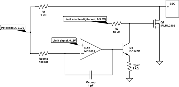
Using the original circuit, you might be able to stabilize that loop just by adding a relative large capacitor (e.g., >1nF) from the drain of Q2 to the Pot readout node. That, together with the Thevenin resistance around your pot, will introduce an extremely low frequency pole (it will be Miller multiplied by a factor of >>1 million) that will only be active during limiting, thus compensating the loop without impacting desired performance. Your other solution, that adds even more amplifiers in the loop, will just make it worse.

Edit: After looking at it more closely, I realized that adding a pole in that location would make things worse as it directly applies the whole gain in the feedback path of the amplifier. So adding it across the op-amp is the way to go. I have updated the schematic to reflect this.

If OA2 is unity gain compensated, you just have to add a pole that is ~< 0.1*op amp compensation pole (GBW/gain) the only issue will become response time. To reduce the need for compensation by reducing the gain, add an emitter resistor to Q1.

I have incorporated both ideas into the following circuit modification. You don't have to combine all of them.

  • Rgain reduces the loop gain by making the gain of Q1 ~ 10
  • Ccomp and Rcomp together introduce a compensation pole whose frequency will be given by w = Ccomp * OpAmpGain * Rcomp. The addition of Rcomp removes the dependency of this pole on the potentiometer value.

schematic

simulate this circuit – Schematic created using CircuitLab

Alternative

But you could considerably reduce your circuit complexity and probably increase reliability by building your limit comparator from scratch. Something like this:

schematic

simulate this circuit

Make sure that the transistors have low Threshold (you can get all of those, well-matched, in a single array). It is just a differential pair with an added gain from the output stage. This makes it intrinsically stable as it is only a 2-stage amplifier.

I added an indicator LED because transistor arrays would have 4 transistors in them. It's biased awkwardly as its intensity depends on R2, but it's free. It can be made a more conventional quasi-digital on/off by adding 2 resistors...

Implementing an option

You can achieve an intermediate solution that somehow approaches your multiplication option by reducing the gain of the loop (for example by reducing R8 or adding source-degeneration resistors on the differential pair). It is a non-linear dependency, but the output will still track the value of the potentiometer with a degree of compression set by the gain and the value of Vlimit.

Scaling to a 3.3V supply

Of course, by changing the values of the resistors and using transistors with a low enough threshold (<1V), it is possible to scale down the supply. The main issue is given by the divider of R3 & R4, this sets the worst-case bias of the differential pair. With a 5V input, the worst case, this divider should probably provide ~2V, leaving 1.3V for the MOSFET Vthreshold and defining the minimum current through R1.

\$\endgroup\$
5
  • \$\begingroup\$ Can you please elaborate more on the compensation suggestion, because I tried it using Draft 2 as a base and it didn't work and I'm pretty sure I'm not following the idea correctly, as you probably implied something else. As for your rolling my own limit comparator it is unfortunately at odds with other design constraints. \$\endgroup\$
    – anrieff
    Commented Dec 11, 2018 at 19:47
  • \$\begingroup\$ @anrieff I edited that section. That should clarify things. \$\endgroup\$ Commented Dec 11, 2018 at 20:33
  • \$\begingroup\$ Hmm, I tried simulating your circuit in LTspice (I finally got to install it) and it oscillates heavily at ~50kHz when the limit is on. I'm only using ADA4661-2 instead of MCP601 in the simulation as my version of LTspice didn't have the MCP601. \$\endgroup\$
    – anrieff
    Commented Dec 12, 2018 at 8:38
  • \$\begingroup\$ @anrieff I guess the phase margin is much worse than I thought. Place the capacitor between the negative input and the output of the op amp instead. \$\endgroup\$ Commented Dec 12, 2018 at 12:23
  • \$\begingroup\$ I had to tweak it a bit, as the capacitor needs to be much smaller in that case (10-33 nF), but otherwise works perfectly, and its response is better than the updated Draft 2, so I'll use this one. Thanks! \$\endgroup\$
    – anrieff
    Commented Dec 12, 2018 at 13:54
1
\$\begingroup\$

Core question: how to stabilize this feedback loop and prevent any oscillations?

Quick reminder of the theory: "generally" a feedback loop is stable if there is enough margin for the frequency where the closed loop gain is 1 (there are special cases where this simple rule is not valid).

In practice, most Opamps are internally compensated and will have a minimum closed loop gain which is typically 0.1. Generally this is in the datasheet, but it it not mentionned for your MCP601. However it is a low bandwidth OPA so it is quite likely compensated.

The two OPAs are mounted as followers.

You are introducing issues that you antipated with the transistor and the mosfet: both add open loop gain. An input voltage swing at the input of the NPN is amplified at its output. The same is true for the N-Channel Mosfet.

By increasing the open loop gain, the internal compensation of the OPA is likely no longer sufficient. Your reflex is to add a capacitor somewhere to add compensation. That is not the easy way to go.

My suggestion is to replace the transistor and the MOSFET with a PNP device and a P-Channel device. Use the Emitter of the PNP as the output instead of the Collector. For the MOSFET, use the Source as the output instead of the Drain.

The PNP output (Emitter) will follow the input (Base) and therefore not introduce any voltage amplification.
Similarly, the MOSFET Gate and Source voltage almost follow each other and introduce no (significant) gain.

As a result the stability of the loop is not impacted, and you do not need to add any extra compensation.

You'll need to rework the current limiting circuit a bit, but that should be quite achievable and possibly even simplify the circuit.

I found the main reason that the schematic was not ok: the feedback was incorrect. In the below amended schematic the digital output to enable/disable the limiter should be 3.3V to disable and high impédance (or input) when enabled. When it is 3.3V, it pulls the gate high so that the MOSFET will not conduct. The circuit can be simulated. The voltage sources simulate changing set points for the operator setting and limiter setting. The On/Off voltage generator does nothing here, I did not find a component to have a tristate output.

I think the schematic can be better, but I followed the one from the question in order to demonstrate the solution with regards to stability.

schematic

simulate this circuit – Schematic created using CircuitLab

Bonus:

The next schematic is not fully ok, but suggests how the MOSFET could be a switch between the input voltage and the limiter voltage. The MOSFET selection must be improved or an analog multiplexer could be used. The limiter voltage is an ideal source here, but it should be buffered in an actual implementation.

schematic

simulate this circuit

\$\endgroup\$
5
  • \$\begingroup\$ Can you please elaborate, as I tried simulating your proposal and it doesn't work, so it is either that I didn't follow your idea correctly, or because my supply rail is 3.3V, so the PMOS is always conducting. I'll add this detail in my question. \$\endgroup\$
    – anrieff
    Commented Dec 5, 2018 at 22:17
  • \$\begingroup\$ @anreief The schematic has been updated. \$\endgroup\$
    – le_top
    Commented Dec 6, 2018 at 18:37
  • \$\begingroup\$ I think this is a great answer, which I'm unfortunately unable to use as it relies on OA2 being fed by split-rails supply (I think the negative rail should go to at least -0.65-Vth_of_PMOS). However, +1 for the approach to reduce amplification, this wouldn't have occurred to me. \$\endgroup\$
    – anrieff
    Commented Dec 11, 2018 at 19:37
  • \$\begingroup\$ Thank your for the acknowledgement.Unfortunately solving the stability issue is not helping with the limiter goal in your topology. ** I looked at it again - it may work if you make the NMOS a switch (short-circuit) between your ESC input and the limiting voltage. \$\endgroup\$
    – le_top
    Commented Dec 12, 2018 at 22:31
  • \$\begingroup\$ I added one extra schematic to make a suggestion for my previous comment. It still needs some work (possibly just a better NMOS selection or an analog switch). \$\endgroup\$
    – le_top
    Commented Dec 12, 2018 at 23:43
0
\$\begingroup\$

Thanks for the good interaction via comments to your question in order to better understand the working conditions and desired behavior of your proposed control circuit.

Here is a simple implementation of ESCin=5 volts * %V{limit} * %R1 as we discussed via comments:

schematic

simulate this circuit – Schematic created using CircuitLab

One very important detail is that whatever I add should not be able to generate a phantom signal, i.e. Vout MUST be always less or equal to Vin, even in the event of software bugs and reasonable hardware failures.

It certainly meets this requirement. The only failure mode is if Vlimit has the possibility of exceeding 5 volts.

A potential disadvantage of this circuit is that the operator control range rescales. But since the operator's feedback is sensory, this may have minimal impact, particularly if you can ramp in your Vlimit control voltage via your DAC.

Another version of this would be to take the wiper output of the pot, resistively scale it if necessary, and then use that as the Vref for the DAC. You can also add common mode decoupled buffers as necessary to ensure low noise inputs throughout.

\$\endgroup\$
3
  • \$\begingroup\$ Unfortunately my device could be turned off, in which case it is desired that the pot control works as if my device didn't exist. In that case, there'd be noone generating Vlimit_in to the pot. I don't have a 5V rail in my device, too, and I don't want to use the 5V from the cable to the pot. In general, I think the "add a resistor in the signal line, and add programmable pull-down circuitry on the ESC side" is the best approach for this project for a number of reasons. \$\endgroup\$
    – anrieff
    Commented Dec 5, 2018 at 21:30
  • \$\begingroup\$ Ok, good additional information. What is the output impedance of your DAC? \$\endgroup\$
    – Glenn W9IQ
    Commented Dec 5, 2018 at 21:40
  • \$\begingroup\$ It is the PIC MCU built-in peripheral, so it can be either the resistor string (high-impedance, I think 200k worst-case for the mid-point value), or that, but buffered by the built-in opamp (so RRIO opamp-grade, say 20-ish ohms, but degrades near the rails). \$\endgroup\$
    – anrieff
    Commented Dec 5, 2018 at 22:24

Your Answer

By clicking “Post Your Answer”, you agree to our terms of service and acknowledge you have read our privacy policy.

Not the answer you're looking for? Browse other questions tagged or ask your own question.