I am designing a pretty straight-forward voltage doubler at 5.8 GHz with MACOM's MA4E1317 diode, which I have used before and know from previous experience that matches pretty well with the spice model they provided.
A block diagram of the circuit is shown below:
The RF signal is a pure tone generated by a siggen.
The matching circuit is determined empirically with a PNA at measurement to make sure that the return loss is greater than 10 dB. In simulation ideal elements were used to populate the PI network so that good return loss was obtained.
The two capacitors were basically chosen to be large enough.
Rload equals 40k Ohm and was chosen to obtain peak efficiency when the input power level is around -3 dbm.
The circuit was built on a two-layer FR-4 substrate with a thickness of ~57 mil.
I used circuit models from vendors for all the components, modelled the pads (0201 and diode) with microstrip lines.
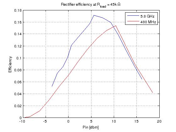
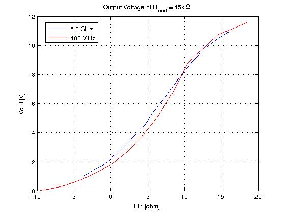
In simulation, I was able to obtain around 70% of peak efficiency at around -3 dbm, in which case I expect to see at least around 3V across the load. However, when I measured the circuit, I was only getting about 1.3 V across the load at -3 dbm, despite the circuit was pretty well matched (S11 < -10 dB).
The simulation was done in ADS with harmonic analysis with an order of 8.
Since this is such a straight forward topology, I am absolutely out of ideas of what could have caused the problem - I built a prototype at a much lower frequency (480 MHz), but I am seeing a similar behavior, thus I am ruling out that this is caused by the parasitics by the pads or unexpected losses from the dielectric.
Could the fact that the caps are beyond their self resonant frequency be the cause of problems, even though it should have been captured in the vendor models?
Here are the measurement data:


